Organic light emitting device

a light-emitting device and organic technology, applied in the direction of organic semiconductor devices, discharge tubes/lamp details, discharge tubes luminescnet screens, etc., can solve the problems of color coordinate shift and light color change with thickness, and achieve the effect of improving the white balance of the oled and attenuating the light intensity, reducing optical interference, and increasing thickness

Inactive Publication Date: 2006-07-27
AU OPTRONICS CORP
View PDF5 Cites 2 Cited by
  • Summary
  • Abstract
  • Description
  • Claims
  • Application Information

AI Technical Summary

Benefits of technology

[0010] Accordingly, the object of the invention is to prevent the OLED from the optical interference, specially, without additional process but by increasing the thickness between the emissive material layer and the two electrodes of the OLED.
[0011] It is another object of the present invention to improve the white balance of the OLED and the attenuation of the light intensity by reducing the optical interference.
[0012] The present invention provides an OLED includes a transparent electrode, a reflective electrode, and an organic light emitting element. The organic light emitting element is disposed between the transparent and the reflective electrode, and has at least one emissive material layer. Note that the thickness between the emissive material layer and the reflective electrode is greater than the major wavelength of light emitted by the OLED so as to avoid the optical interference.
[0013] The present invention can be applied to at least four types OLED such as a bottom emission, an inverted bottom emission, a top emission and an inverted top emission. Besides, it can be also applied to avoid the optical interference occurring between the emission material layer and the transparent.

Problems solved by technology

In practice, the variation of the viewing angle affects the interference band sensed by an eye, and results in the color coordinates shift.
Specially, the optical interference can result in the light color change with the thickness when the light transports between the emissive material layer and the reflective electrode.

Method used


Image

  • Organic light emitting device
  • Organic light emitting device
  • Organic light emitting device

Examples


Embodiment Construction

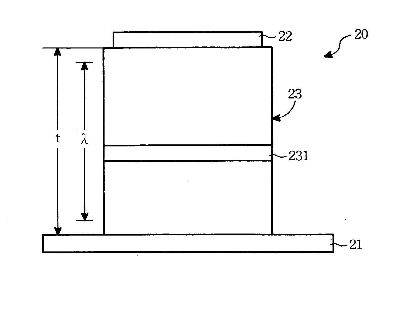
[0032] Refer to FIG. 2, the OLED 20 of the present invention includes a transparent electrode 21, a reflective electrode 22, and an organic light emitting element 23. The organic light emitting element 23 is interposed between the transparent electrode 21 and reflective electrode 22, and includes at least one emissive material layer 231 that is doped with an emissive dopant. It is emphasized that the organic light emitting element 23 has a thickness t greater than the major wavelength λ of light emitted by the OLED 20. Because the wavelength of the visible light is from 380 to 700 nm, the thickness t of the organic light emitting element 23 can be reasonably defined as 380 to 10000 nm. Under the reasonable thickness, the absorbance of the light can be also controlled.

[0033] The OLED has four types such as the bottom emission, the inverted bottom emission, the top emission and the inverted top emission. In various types of OLEDs, the reflective electrode may be taken as an anode or ...


PUM


Abstract

An organic light emitting device includes a transparent electrode, a reflective electrode, and an organic light emitting element. The organic light emitting element includes an emissive material layer doped with an emissive dopant, and is disposed between the transparent electrode and the reflective electrode. The total thickness of the organic light emitting element is greater than the wavelength of the light from the emissive material layer.

Description

[0001] This application claims the benefit of Taiwan Application Serial No. 094101891, filed Jan. 21, 2005, the subject matter of which is incorporated herein by reference. BACKGROUND OF THE INVENTION [0002] (1) Field of the Invention [0003] The invention relates to an organic light emitting device capable of reducing optical interference. [0004] (2) Description of the Prior Art [0005] An organic light emitting diode (OLED) is a future trends in development of a flat display for the benefit of lightness, thinness, flexibility, portability, full color, high brightness, power saving, wide viewing angle, and low image sticking. The OLED includes an inverted type and a non-inverted type. The inverted type means that a manufacturing process of the OLED initiates with forming a cathode on a substrate. Refer to FIG. 1A that shows a conventional structure of an inverted OLED. A transparent electrode 12, an electron transport layer 13, an emissive material layer (EML) 14, a hole transport la...

Claims


Application Information

Patent Timeline
Patent Type & Authority Applications(United States)
IPC IPC(8): H01L51/52H05B33/12
CPCH01L51/5262H01L2251/558H10K50/85H10K2102/351
Inventor LI, SHI-HAOCHEN, CHE-JEN
Owner AU OPTRONICS CORP
Why Eureka
Try Eureka