Photo-electric conversion apparatus with alternating photoelectric conversion elements

a technology of photoelectric conversion elements and conversion apparatus, which is applied in the field of photoelectric conversion element array, can solve the problems of optical waveguide, inability to adopt the method to mass production, and difficulty in further raising the density of the array of core layers, so as to achieve sufficient distance, avoid optical and electrical interference and crosstalk effectively, and facilitate the effect of mounting

Active Publication Date: 2009-11-24
SONY CORP
View PDF14 Cites 3 Cited by
  • Summary
  • Abstract
  • Description
  • Claims
  • Application Information

AI Technical Summary

Benefits of technology

[0018]The present invention was conceived in order to solve the above-described problems, and an object thereof is to provide a photoelectric conversion element array, not only allows high-density integration of optical interconnects, but also reduces optical interference or crosstalk due to the photoelectric conversion element, and can thereby provide a photoelectric conversion element array allowing efficient propagation of light, an integrated apparatus thereof, a mounted structure of them, and an optical information processing apparatus.
[0023]The present inventor has extensively been investigating through the above-described integration with a higher density, and has already proposed, in Japanese Patent Application Publication No. 2002-364841 (occasionally referred to as “the earlier application”, hereinafter), an optical waveguide having a plurality of core layers arranged in parallel, wherein positions of the light input / output sections are shifted from those of every adjacent core layer in the direction of guiding of light, and have first found out that this sort of structure can be realized by a synchrotron radiation lithographic process. This process makes it possible to arrange also the photoelectric conversion elements (emitting optics and receiving optics), arranged as being corresponded with the light input / output portions of the core layers, as being shifted in the direction of guidance of wave. As a consequence, the distance between the adjacent emitting optics (or receiving optics) can be widened as compared with the above-described conventional example, even under a high integration density, so that adverse influences, such as light interference between the adjacent photoelectric conversion elements, crosstalk due to heat generation by the elements and so forth, can be reduced as compared with the structure according to the prior art.
[0025]In contrast, the photoelectric conversion element array of the present invention is composed of a plurality of photoelectric conversion elements (emitting optics or receiving optics) arranged in an array, wherein the photoelectric conversion elements are arranged alternately at different positions so that every second one is aligned on the same line in the direction of array, so that a sufficient level of distance can be ensured between every adjacent photoelectric conversion elements even if the integration density is increased. Difficulty in the mounting can therefore be moderated, and optical and electrical interferences and crosstalk are effectively be avoidable, allowing further pursuit of larger transmission capacity and lower cost of the system.

Problems solved by technology

However, the optical waveguide 51 according to the prior art described in the above suffers from a technical difficulty in further raising the density of array of the core layers 57 (typically to 100-μm pitch or below).
Although selective formation of the mirror portions typically by isotropic etching has been investigated, it is supposed at present as impossible to adopt the method to mass production, due to insufficient levels of accuracy and stability.

Method used


Image

  • Photo-electric conversion apparatus with alternating photoelectric conversion elements
  • Photo-electric conversion apparatus with alternating photoelectric conversion elements
  • Photo-electric conversion apparatus with alternating photoelectric conversion elements

Examples


first embodiment

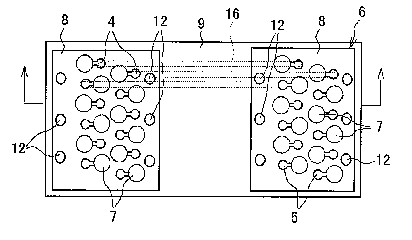
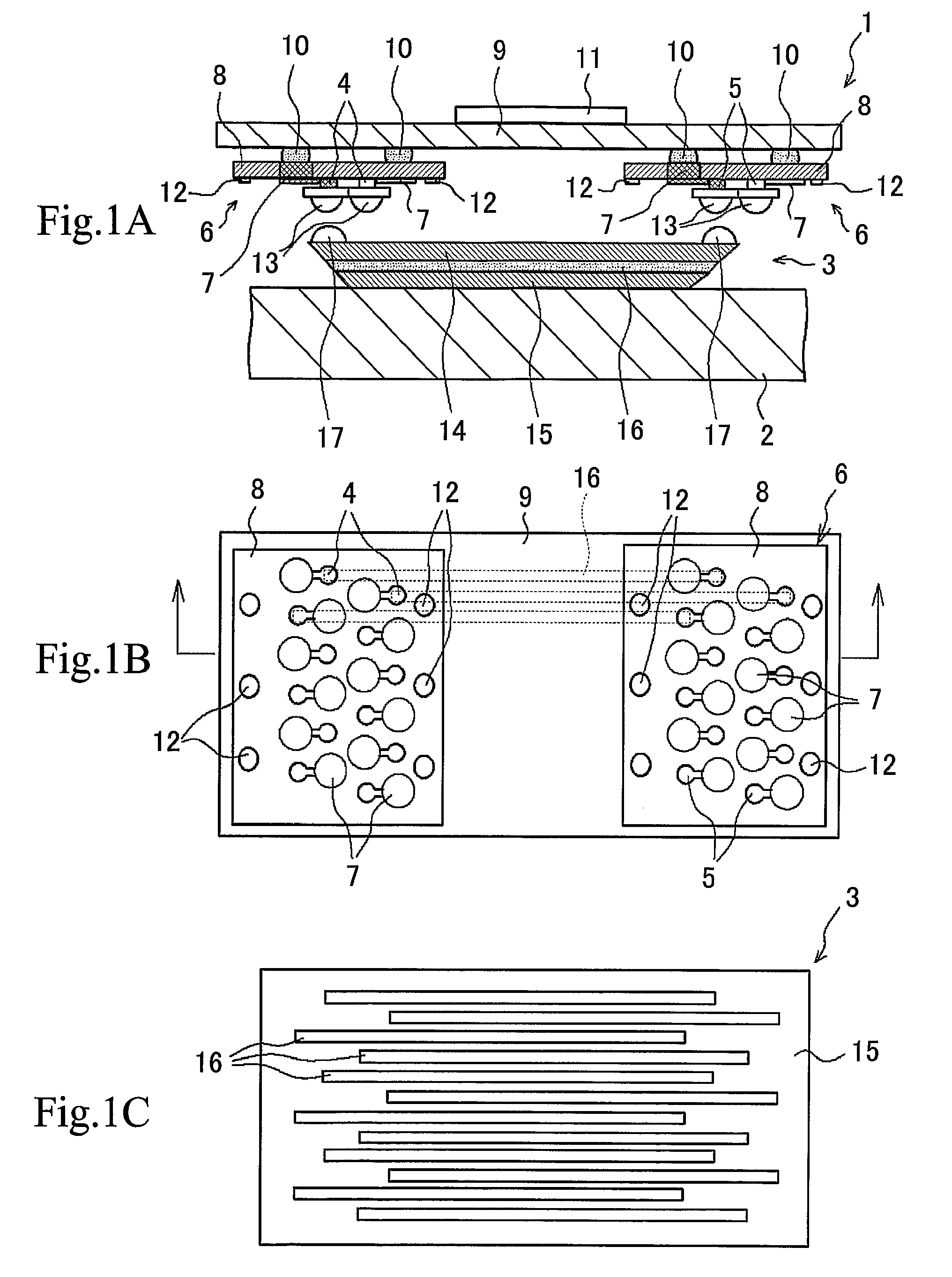
[0039]FIG. 1A to FIG. 1C are schematic drawings showing a photoelectric conversion element array integrated apparatus and an optical information processing apparatus based on the present invention. As shown in FIG. 1A, an optical information processing apparatus 1 based on the present invention has an optical waveguide 3 formed on a printed wiring board 2, in which light modulated by signals by the emitting optics (surface emission laser, for example) 4 as the photoelectric conversion element is introduced into the optical waveguide 3, guided through the optical waveguide 3, emitted from the optical waveguide 3, and received by the receiving optics (photodiode, for example) 5 as the photoelectric conversion element. In this way, an optical transmission / communication system using the optical waveguide 3 as a transmission path of signal-modulated laser light and so forth can be configured.

[0040]As shown in FIG. 1A and FIG. 1B, a photoelectric conversion element array integrated appara...

second embodiment

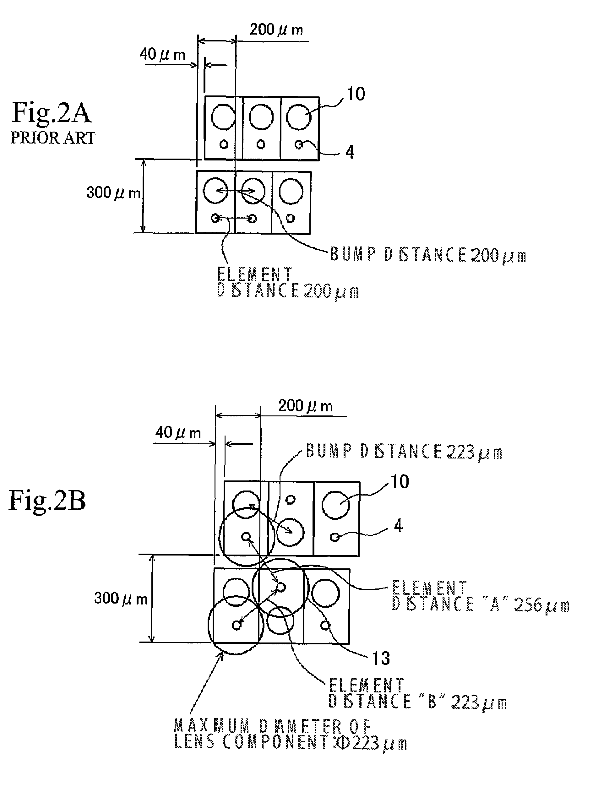
[0058]In order to further increase the distance between the adjacent photoelectric conversion elements 4, 5, it is also allowable in the photoelectric conversion element array based on the present invention, as shown in, to shift every second photoelectric conversion element aligned in the direction of array, towards the direction of guiding of light (as much as 26 μm, for example). By this configuration, the element distance “A” between the photoelectric conversion element array (and distance between the adjacent solder bumps 10) can be set to 236 μm, and the element distance “B” in the same photoelectric conversion element array can be set to 236 μm, still larger than in the exemplary arrangement of the first embodiment shown in FIG. 2B. Moreover, the maximum lens component 13 can be ensured to as much as 236 μm, making it still larger than in the exemplary arrangement according to the first embodiment as shown in FIG. 2B. In this way, the coupling efficiency of light can further ...

third embodiment

[0059]As described in the above, the optical information processing apparatus based on the present invention has the photoelectric conversion element arrays and the optical waveguide opposing to the photoelectric conversion element arrays, and is preferably applicable, for example, to a structure having a socket and an optical waveguide disposed in the socket, although the structure thereof is appropriately selectable without departing from the spirit of the present invention.

[0060]FIG. 4A and FIG. 4B are schematic perspective views of the socket. FIG. 4A is a schematic perspective view as viewed from the side of the surface on which the optical waveguide of the socket is disposed, and FIG. 4B is a schematic sectional view as viewed from the side of the surface opposite to that shown in FIG. 4A.

[0061]As shown in FIG. 4A and FIG. 4B, a socket 20 has a positioning means composed of an irregularity structure for positioning and fixing the optical waveguide formed therein. More specific...


PUM


Abstract

A photoelectric conversion element array having a plurality of photoelectric conversion elements (emitting optics 4, receiving optics 5) arranged in an array, and the photoelectric conversion elements 4, 5 are arranged alternately at different positions so that every second one is aligned on the same line in the direction of array. A mounted structure of photoelectric conversion element array, having the emitting optics array and the receiving optics array in the photoelectric conversion element array of this invention, arranged on an interposer substrate 9 so as to oppose therewith, and these arrays are mounted on the interposer substrate 9 through the external connection terminals 7. An optical information processing apparatus 1 having the photoelectric conversion element array of the present invention, and an optical wave guide 3 opposed to the respective optics of the photoelectric conversion element arrays. These configurations not only allow high-density integration of optical interconnects, but also reduce optical interference or crosstalk due to the photoelectric conversion element, and can thereby provide a photoelectric conversion element array allowing efficient propagation of light, an integrated apparatus thereof, a mounted structure of them, and an optical information processing apparatus.

Description

TECHNICAL FIELD[0001]This invention relates to a photo-electric conversion element array, an integrated apparatus of the same, mounted structures of them, and an optical information processing apparatus.BACKGROUND ART[0002]Nowadays, all signal propagations among semiconductor chips such as LSIs (large scale integrated circuits) rely upon electric signals via interconnections on a substrate. However, with recent trends in higher functionalization of MPU, volume of data transmission among the chips has extremely increased, and this has raised various high-frequency-related problems. Representative problems include RC signal delay, impedance mismatching, EMC / EMI, crosstalk and the like.[0003]In order to solve the above-described problems, various techniques such as optimization of interconnect arrangement, development of new materials and so forth have been adopted to the solution, mainly contributed by mounting-related industries.[0004]However in recent years, effects of the above-des...

Claims


Application Information

Patent Timeline
Patent Type & Authority Patents(United States)
IPC IPC(8): G01J1/42H01J40/14H04N3/14G02B6/42G02B6/43H01L25/16H01L31/0232H01L31/12H01L31/167H01L33/08H01L33/58H01S5/022
CPCG02B6/43H01L31/167G02B6/4206G02B6/4214H01L25/167H01L2924/0002H01L2924/00
Inventor OHTORII, HIIZU
Owner SONY CORP
Why Eureka
Try Eureka