Semiconductor Device with Field Electrode Structures in a Cell Area and Termination Structures in an Edge Area

Active Publication Date: 2016-03-03
INFINEON TECH AUSTRIA AG
View PDF3 Cites 12 Cited by
  • Summary
  • Abstract
  • Description
  • Claims
  • Application Information

AI Technical Summary

Problems solved by technology

Higher dopant concentrations in turn reduce the on state resistance of the device.
During fabric

Method used


Image

  • Semiconductor Device with Field Electrode Structures in a Cell Area and Termination Structures in an Edge Area
  • Semiconductor Device with Field Electrode Structures in a Cell Area and Termination Structures in an Edge Area
  • Semiconductor Device with Field Electrode Structures in a Cell Area and Termination Structures in an Edge Area

Examples


Embodiment Construction

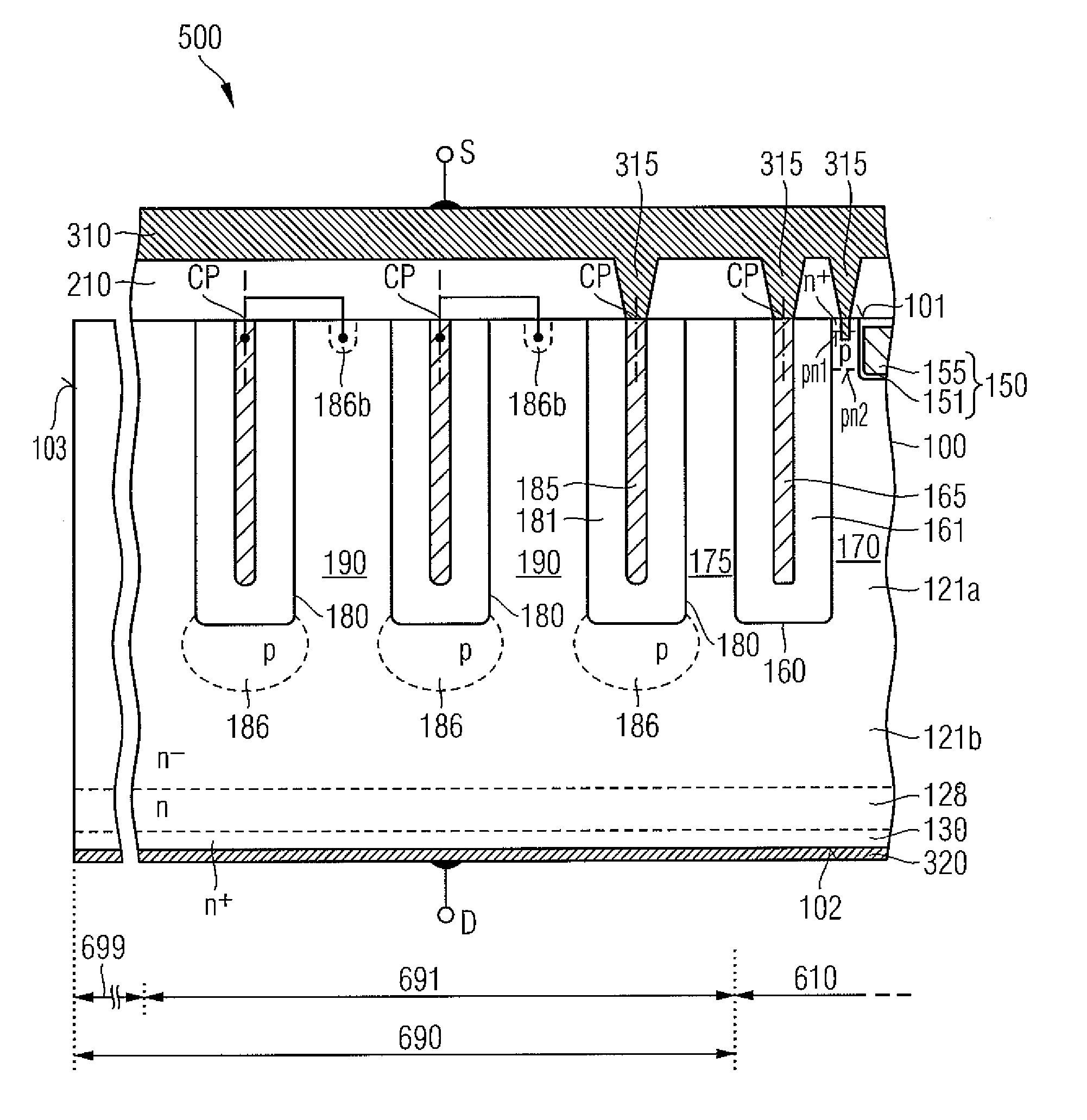
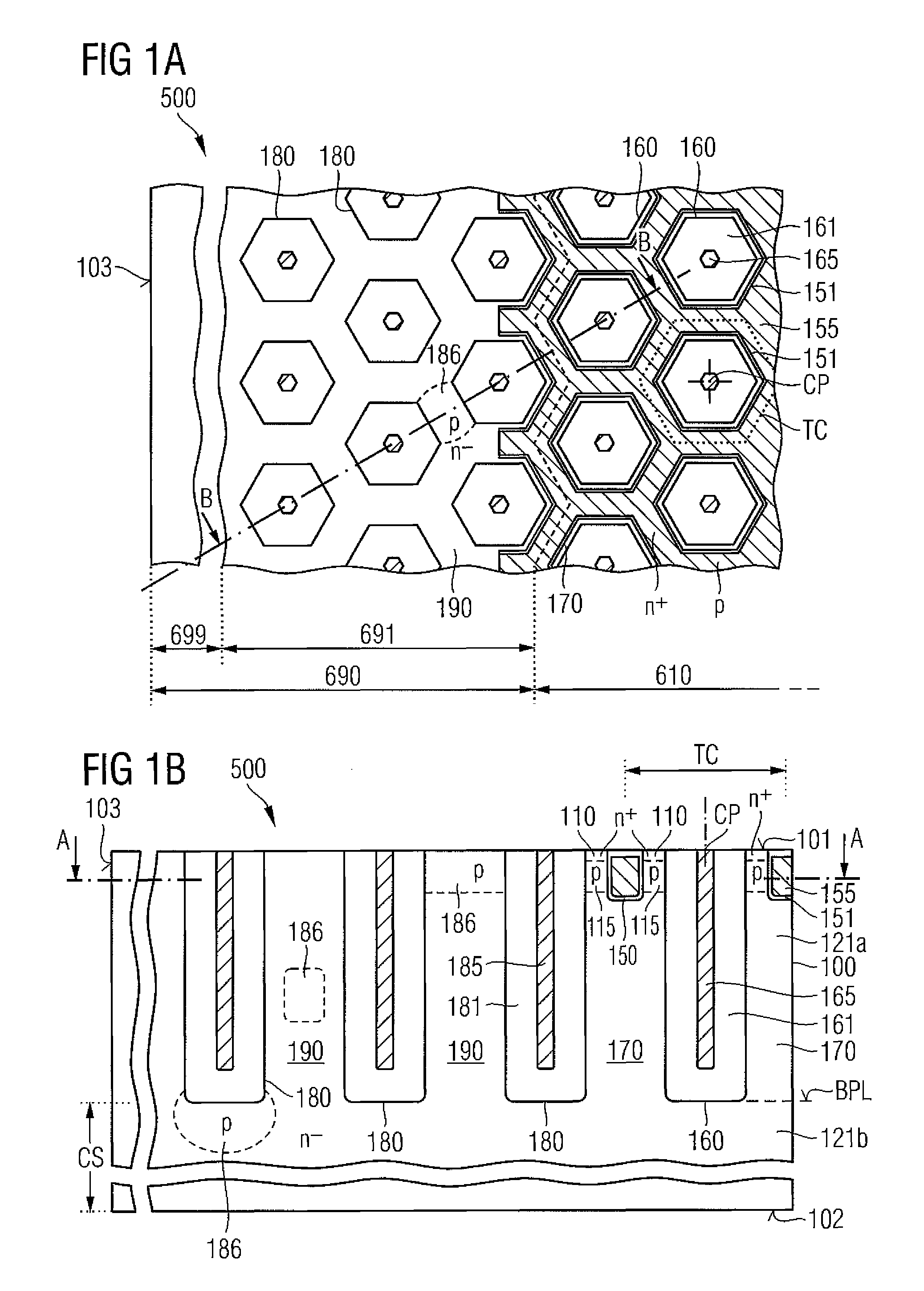
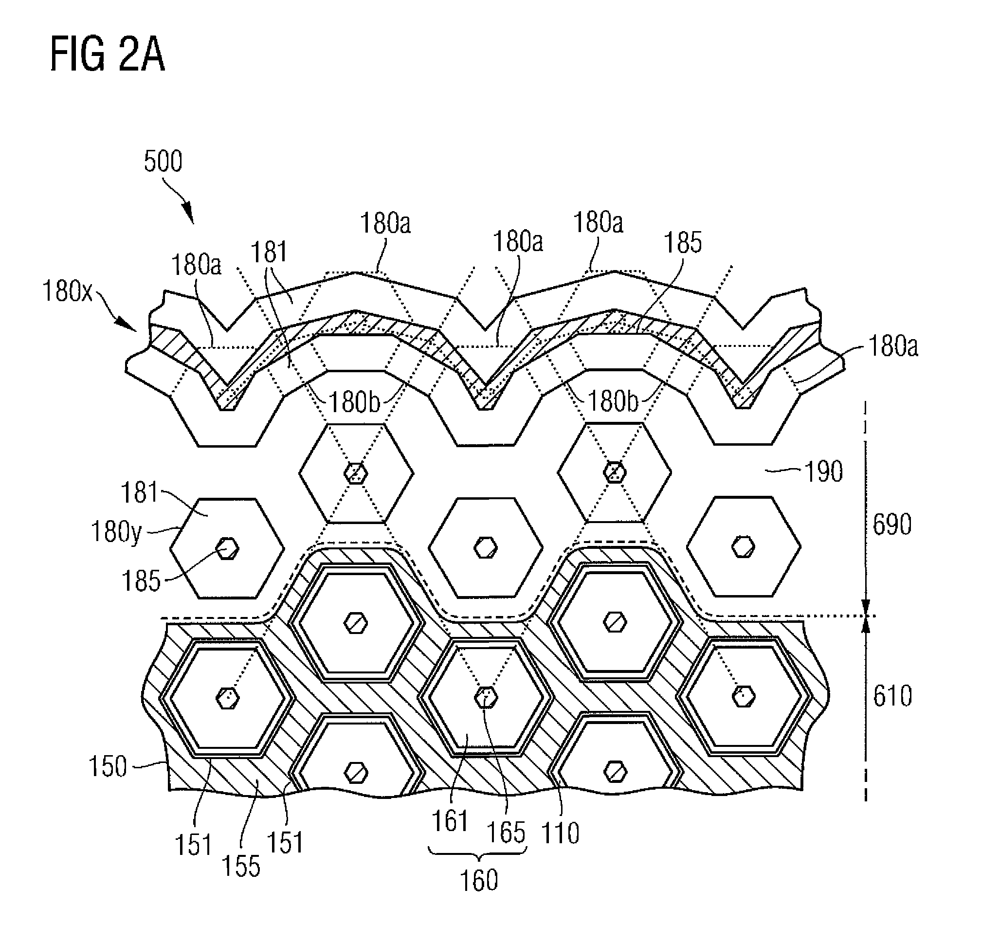
[0031]In the following detailed description, reference is made to the accompanying drawings, which form a part hereof and in which are shown by way of illustrations specific embodiments in which the invention may be practiced. It is to be understood that other embodiments may be utilized and structural or logical changes may be made without departing from the scope of the present invention. For example, features illustrated or described for one embodiment can be used on or in conjunction with other embodiments to yield yet a further embodiment. It is intended that the present invention includes such modifications and variations. The examples are described using specific language, which should not be construed as limiting the scope of the appending claims. The drawings are not scaled and are for illustrative purposes only. For clarity, the same elements have been designated by corresponding references in the different drawings if not stated otherwise.

[0032]The terms “having”, “contai...


PUM


Abstract

A semiconductor device includes field electrode structures regularly arranged in lines in a cell area and forming a first portion of a regular pattern. Termination structures are formed in an inner edge area surrounding the cell area, wherein at least portions of the termination structures form a second portion of the regular pattern. Cell mesas separate neighboring ones of the field electrode structures from each other in the cell area and include first portions of a drift zone, wherein a voltage applied to a gate electrode controls a current flow through the cell mesas. At least one doped region forms a homojunction with the drift zone in the inner edge area.

Description

BACKGROUND[0001]The present application claims priority under 35 USC §119 to German (DE) Patent Application Serial No. DE 10 2014 112 371.9 filed on Aug. 28, 2014. The disclosure in this priority application is hereby incorporated fully by reference into the present application.BACKGROUND ART[0002]Power semiconductor devices based on IGFET (insulated gate field effect transistor) cells are typically vertical devices with a load current flow between a first surface at a front side of a semiconductor die and a second surface at a rear side. In a blocking mode, stripe-shaped compensation structures extending from the front side into the semiconductor die deplete semiconductor mesas formed between the stripe-shaped compensation structures. The compensation structures allow higher dopant concentrations in the semiconductor mesas without adverse impact on the blocking capability. Higher dopant concentrations in turn reduce the on state resistance of the device. During fabrication, deep co...

Claims


Application Information

Patent Timeline
IPC IPC(8): H01L29/78H01L29/06
CPCH01L29/0696H01L29/7811
Inventor SIEMIENIEC, RALFBLANK, OLIVERHIRLER, FRANZHUTZLER, MICHAELPOELZL, MARTIN
Owner INFINEON TECH AUSTRIA AG
Why Eureka
Try Eureka