Multilayer wiring board

Inactive Publication Date: 2016-03-03
DENSO CORP +1
View PDF0 Cites 11 Cited by
  • Summary
  • Abstract
  • Description
  • Claims
  • Application Information

AI Technical Summary

Benefits of technology

[0020]According to each of the exemplary embodiments, there is provided a multilayer wiring board which mak

Problems solved by technology

In a case where the equalization is performed using a circuit within a semiconductor chip (“active equalization” hereinafter), the operation speed of

Method used


Image

  • Multilayer wiring board
  • Multilayer wiring board
  • Multilayer wiring board

Examples


first embodiment

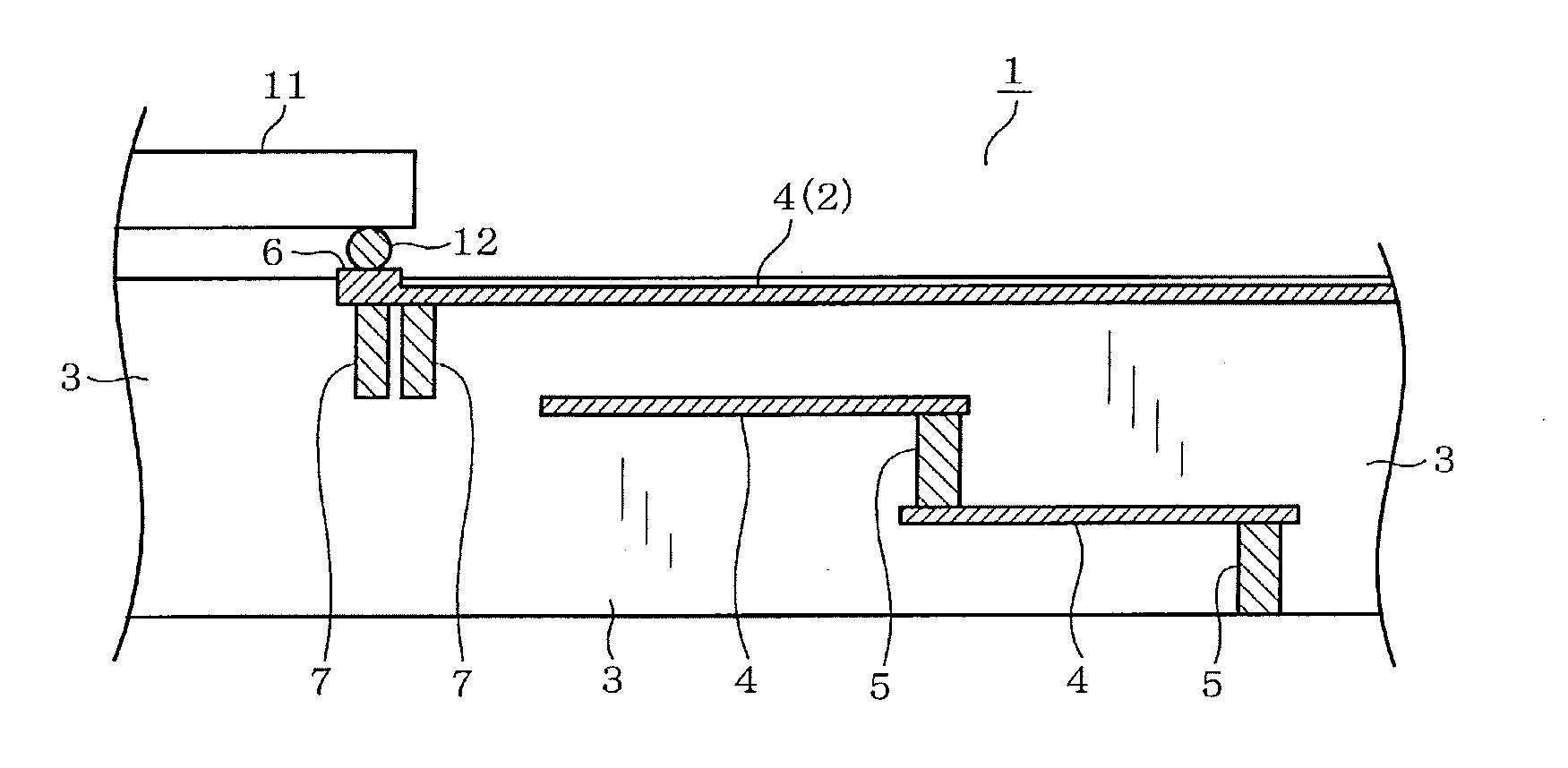
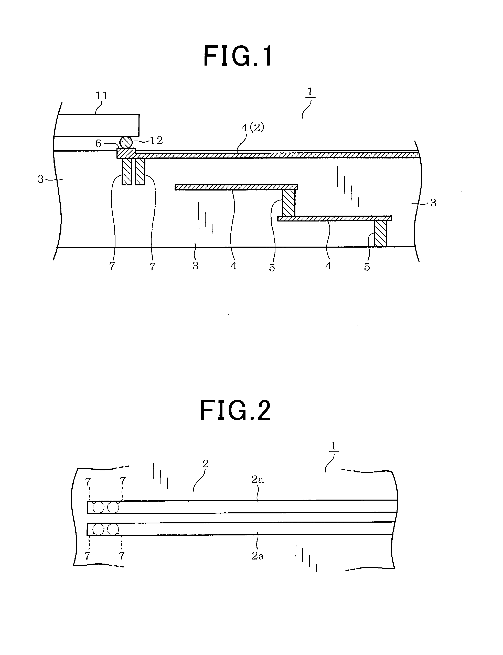
[0032]A multilayer wiring board 1 according to a first embodiment of the invention is described with reference to FIGS. 1 to 5. FIG. 1 is a longitudinal cross-sectional view schematically showing a part of the multilayer wiring board 1. FIG. 2 is a plan view of a differential transmission line 2 provided in the multilayer wiring board 1. The differential transmission line 2 is used for performing signal transmission at a high speed of 10 Gbps to 30 Gbps, for example.

[0033]As shown in FIG. 1, the multilayer wiring board 1 includes insulating layers 3 stacked on one another, each insulating layer 3 being made of thermoplastic resin material, for example. The surface of each of the insulating layers 3 is formed with a surface conductor pattern 4 made of copper foil, for example.

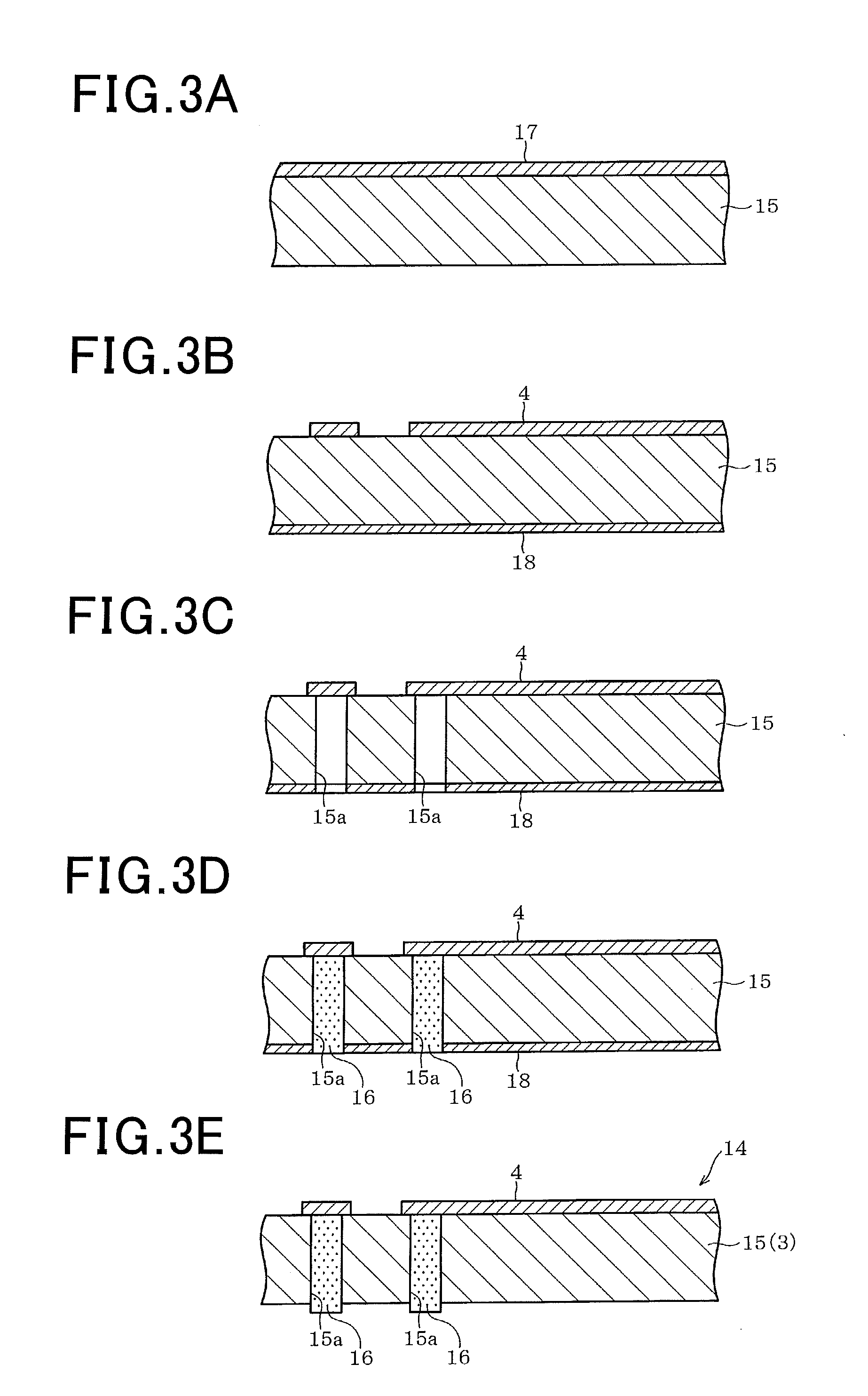
[0034]As described later, the surface conductor pattern 4 includes the differential transmission line 2. The multilayer wiring board 1 is provided with interlayer connecting sections (vias) 5 which vertically co...

fourth embodiments

Second to Fourth Embodiments

[0063]FIG. 6 schematically shows the structure of a multilayer wiring board 21 according to a second embodiment of the invention. The second embodiment differs from the first embodiment in that a differential transmission line 22 is formed within the insulating layer 3. In this embodiment, the differential transmission line 22 extends from the lands 6 along the surface of the multilayer wiring board 21 to the right in FIG. 6 to reach an interlayer connecting section 23, and extends from the interlayer connecting sections 23 to the right within the insulating layer 3. Like in the first embodiment, in this embodiment, the open stubs 7 are provided in the signal transmission end of the differential transmission line 22. The second embodiment provides the same advantages as those provided by the first embodiment.

[0064]FIG. 7 schematically shows the structure of a multilayer wiring board 31 according to a third embodiment of the invention. The third embodiment...


PUM


Abstract

A multilayer wiring board includes an insulating layers stacked on one another, lands formed on an upper surface part of the multilayer wiring board, and a differential transmission line formed on or in each of the insulating layer. An electronic component is mounted on the lands. The differential transmission line is constituted of a pair of signal lines which extend from the lands toward a signal receiving end. Each of the signal lines is provided with an open stub which extends in a stacking direction of the insulating layers, and has a same width as a width of the signal lines, one end of the open stub being connected to a corresponding one of the signal lines, and another end of the open stub being open.

Description

[0001]This application claims priority to Japanese Patent Application No. 2014-174167 filed on Aug. 28, 2014, the entire contents of which are hereby incorporated by reference.BACKGROUND OF THE INVENTION[0002]1. Field of the Invention[0003]The present invention relates to a multilayer wiring board.[0004]2. Description of Related Art[0005]A multilayer wiring board used for information devices with a CPU includes a stack of insulating layers. Each of the insulating layers is formed with a wiring pattern on its upper or lower surface. The wiring patterns of the adjacent insulating layers are electrically connected through vias. For example, refer to Japanese Patent Application Laid-open No. 2008-235338. In such a multilayer wiring board, data transmission between semiconductor chips, for example, between a CPU and a memory or between a CPU and a device connected to the CPU is performed through the wiring patterns.[0006]Recently, the operation speed and data transmission rate of LSIs ar...

Claims


Application Information

Patent Timeline
IPC IPC(8): H05K1/02H05K1/11H05K7/02
CPCH05K1/0245H05K7/02H05K2201/10719H05K1/11H05K1/0298H05K1/0251
Inventor KATAOKA, RYOHEIKONDOH, KOUJIAKIMICHI, JYUNOTSUKA, KANJIAKIYAMA, YUTAKAHASHIMOTO, KAORU
Owner DENSO CORP
Why Eureka
Try Eureka