

Thin film transistor substrate and method of fabricating the same
a technology of thin film transistors and substrates, applied in semiconductor/solid-state device manufacturing, semiconductor devices, electrical devices, etc., can solve the problems of increasing the thickness of increasing the cost of fabricat and difficulty in slimming the liquid crystal display device. to achieve the effect of reducing the cos
- Summary
- Abstract
- Description
- Claims
- Application Information
AI Technical Summary
Benefits of technology
Problems solved by technology
Method used
Image

Examples
first embodiment
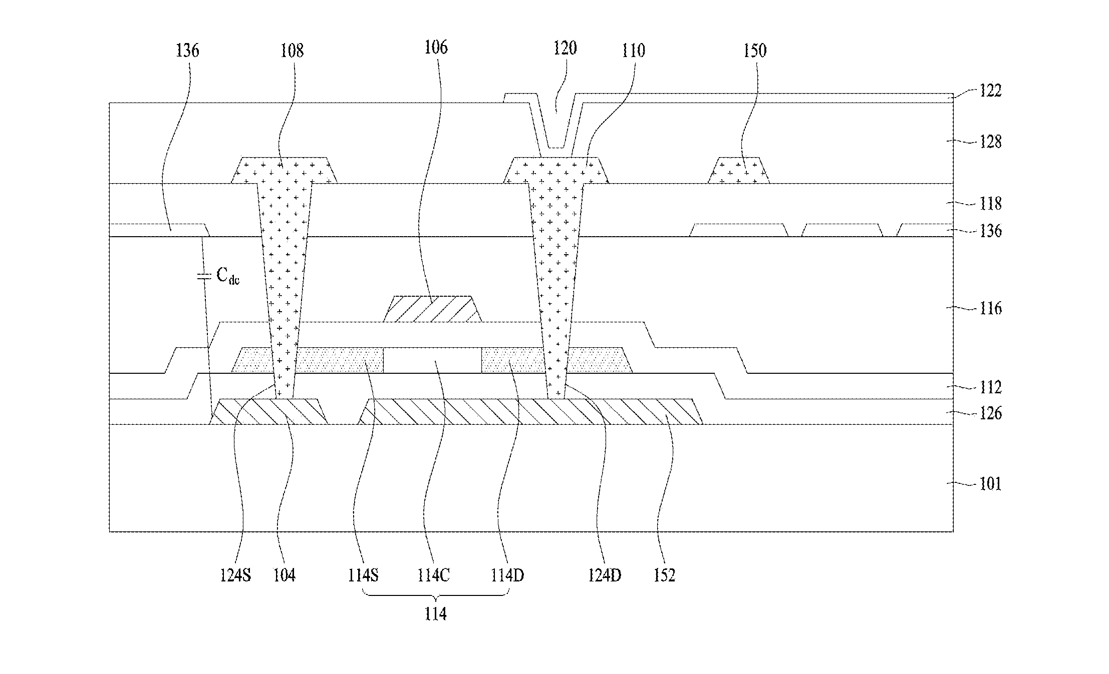
[0034]The passivation film prevents the introduction of external moisture or foreign matter to protect the respective thin films constituting the thin film transistor. The passivation film is formed to have a multi-layer structure. In the present invention, a case in which first and second passivation films 118 and 128 are provided will be described by way of example.
[0035]The first passivation film 118, which is preferably made of an inorganic dielectric material, such as SiNx or SiOx, is formed between the common electrode 136 and the touch sensing line 150 so as to isolate the common electrode 136 and the touch sensing line 150 from each other. The second passivation film 128, which is preferably made of an inorganic dielectric material, such as SiNx or SiOx, is formed between the touch sensing line 150 and the pixel electrode 122 so as to isolate the touch sensing line 150 and the pixel electrode 122 from each other.
[0036]The pixel electrode 122 is formed on the second passivati...
second embodiment
[0061]FIG. 3 is a sectional view showing a thin film transistor substrate according to the present invention.
[0062]The thin film transistor substrate shown in FIG. 3 is identical in construction to the thin film transistor substrate shown in FIG. 1 except that the touch sensing line 150 is formed directly on the common electrode 136 such that the common electrode 136 and the touch sensing line 150 directly contact each other. Accordingly, a detailed description of components of the thin film transistor substrate that are the same will be omitted.
[0063]The touch sensing line 150 shown in FIG. 3, which is made of a material identical to or different from that of the source and the drain contact electrodes 108 and 110, is formed on the common electrode 136. The touch sensing line 150 electrically interconnects common electrodes 136 of adjacent pixel regions such that the common electrodes 136 are used as touch sensing electrodes during a non-display period.
[0064]The touch sensing line ...
third embodiment
[0083]FIG. 5 is a sectional view showing a thin film transistor substrate according to the present invention
[0084]The thin film transistor substrate shown in FIG. 5 is identical in construction to the thin film transistor substrate shown in FIG. 3 except that a first passivation film 138 made of an organic dielectric material is further formed on the interlayer insulation film 116. Accordingly, a detailed description of components of the thin film transistor substrate that are the same will be omitted.
[0085]The first passivation film 138 formed on the interlayer insulation film 116 is made of an organic dielectric material, such as photo acrylic. The first passivation film 138 is formed between the data line 104 and the common electrode 136, which are formed on the substrate 101. As a result, the distance between the data line 104 and the common electrode 136 is greater than in the structure shown in FIG. 3. Consequently, it is possible to further reduce the parasitic capacitance Cd...
PUM
 Abstract
Description
Claims
Application Information