Maskless exposure device, maskless exposure method and display substrate manufactured by the maskless exposure device and the maskless exposure method

a technology of maskless exposure and exposure method, which is applied in the direction of microlithography exposure apparatus, printers, instruments, etc., can solve the problems of increasing the manufacturing cost of the display substrate, affecting the quality of the display substrate, so as to reduce the difference of critical dimensions of adjacent lines, reduce the effect of defects, such as the stain of the display panel, and reduce the manufacturing cost of the mask

Inactive Publication Date: 2016-04-28
SAMSUNG DISPLAY CO LTD
View PDF2 Cites 2 Cited by
  • Summary
  • Abstract
  • Description
  • Claims
  • Application Information

AI Technical Summary

Benefits of technology

[0033]According to the present exemplary embodiment, the pattern extending in a direction parallel to a scan direction of the exposure head has a structure in which the first pattern portion and the second pattern portion are alternately arranged. Thus, the pattern may have a sawtooth shape. Therefore, an effect of different characteristics of beams may be offset so that defects, such as a stain in a display panel, may be reduced.
[0034]In addition, sides of a gate line or a data line of a display panel may be non-uniform in a plan view. Therefore, an effect resulting from different characteristics of various beams may be offset, and a difference of critical dimensions of adjacent lines may be reduced. Accordingly, defects, such as stain of display panel, may be decreased.

Problems solved by technology

As fabricating cost of the mask is relatively high, manufacturing cost of the display substrate may increase.
Accordingly, faults, such as a stain in the display panel, may occur.
A shape of sides of the data lines is non-uniform in a plan view.
A shape of sides of the gate lines is non-uniform in a plan view.
In addition, sides of a gate line or a data line of a display panel may be non-uniform in a plan view.

Method used


Image

  • Maskless exposure device, maskless exposure method and display substrate manufactured by the maskless exposure device and the maskless exposure method
  • Maskless exposure device, maskless exposure method and display substrate manufactured by the maskless exposure device and the maskless exposure method
  • Maskless exposure device, maskless exposure method and display substrate manufactured by the maskless exposure device and the maskless exposure method

Examples


Embodiment Construction

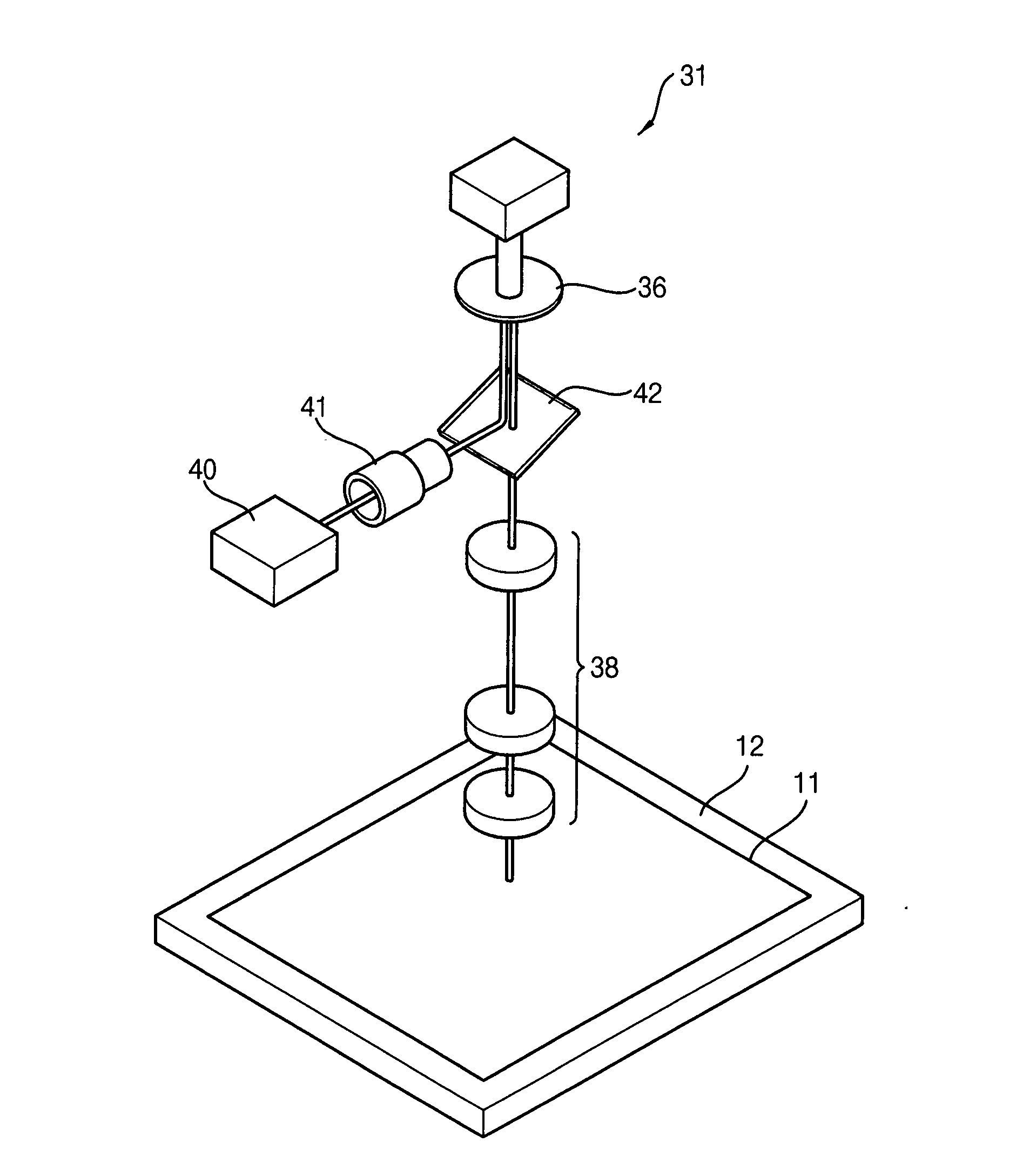
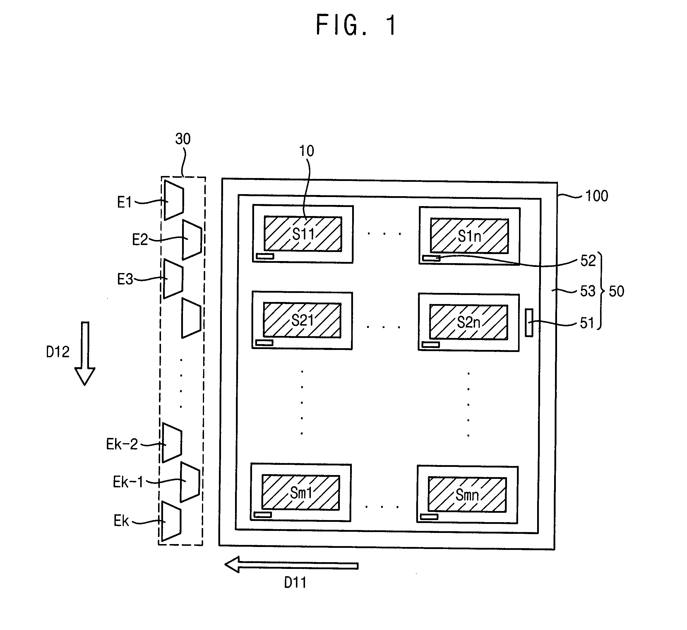
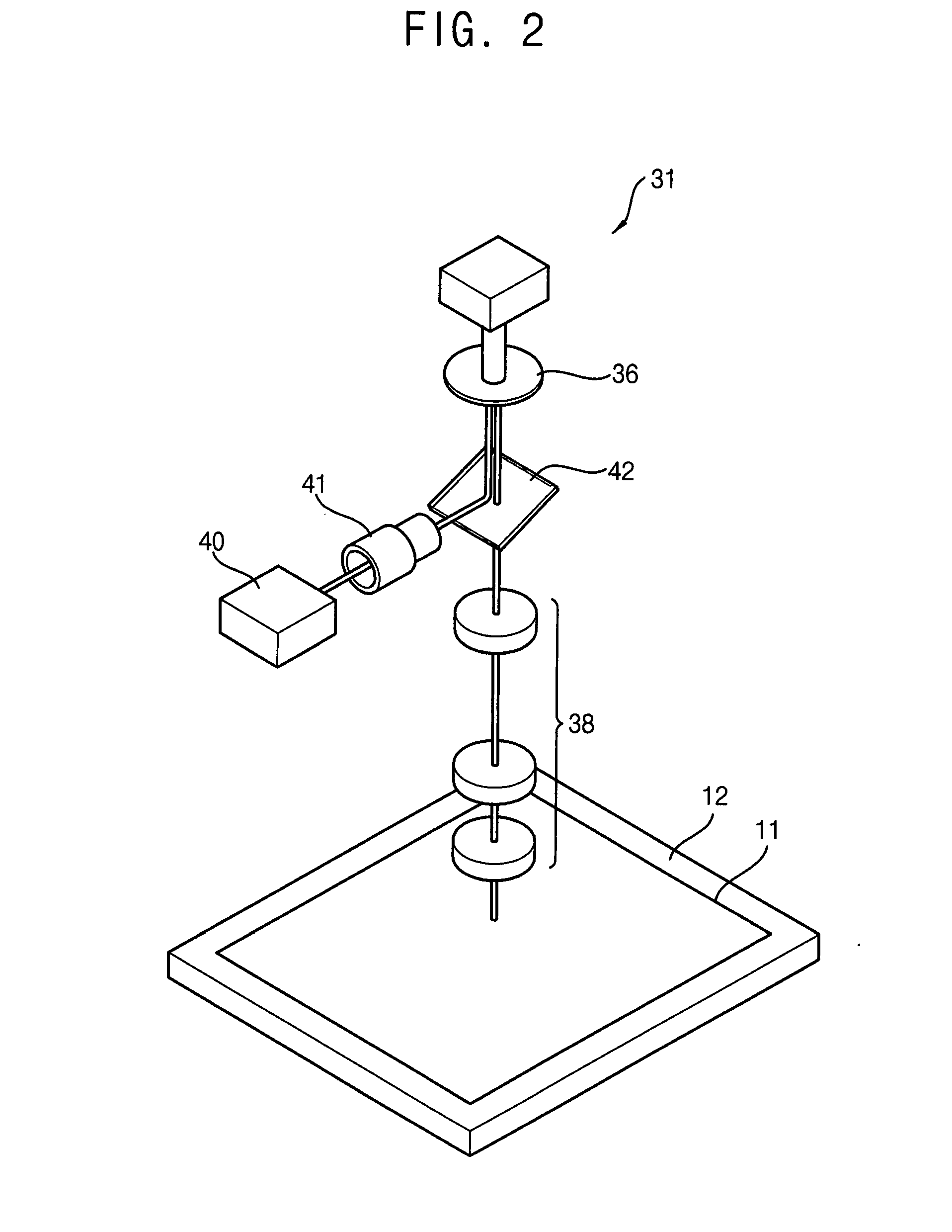
[0049]Hereinafter, exemplary embodiments of the present invention will be explained in detail with reference to the accompanying drawings.

[0050]It will be understood that when an element or layer is referred to as being “on”, “connected to”, or “coupled to” another element or layer, it may be directly on, connected, or coupled to the other element or layer or one or more intervening elements or layers may also be present. When an element is referred to as being “directly on,”“directly connected to,” or “directly coupled to” another element or layer, there are no intervening elements or layers present. For example, when a first element is described as being “coupled” or “connected” to a second element, the first element may be directly coupled or connected to the second element or the first element may be indirectly coupled or connected to the second element via one or more intervening elements. The same reference numerals designate the same elements. As used herein, the term “and / or...


PUM

PropertyMeasurementUnit
widthaaaaaaaaaa
widthaaaaaaaaaa
widthaaaaaaaaaa

Abstract

A maskless exposure device includes an exposure head including a digital micro-mirror device and an exposure source, the digital micro-mirror device being configured to reflect a source beam outputted from the exposure source to a substrate and a system controller configured to control the digital micro-mirror device by using a graphic data system file. The graphic data system file includes data regarding patterns to be formed on the substrate. A pattern extending in a direction parallel to a scan direction of the exposure head includes a first pattern portion having a first width that is greater than a target width and a second pattern portion alternately disposed with the first pattern portion and having a second width that is less than the target width.

Description

CROSS-REFERENCE TO RELATED APPLICATION[0001]This application claims priority to and the benefit under 35 U.S.C. §119 of Korean Patent Application No. 10-2014-0145417, filed on Oct. 24, 2014 in the Korean Intellectual Property Office KIPO, the content of which are hereby incorporated by reference in its entirety.BACKGROUND[0002]1. Field[0003]Exemplary embodiments of the present invention relate to a maskless exposure device, a maskless exposure method, and a display substrate manufactured by using the maskless exposure device and the maskless exposure method.[0004]2. Description of the Related Art[0005]Generally, to form a metal pattern of thin film transistors (“TFTs”), which are switching elements of a display substrate, and signal lines, a metal layer and a photoresist layer are sequentially formed and a mask corresponding to the metal pattern is disposed on the photoresist layer.[0006]Then, a light is irradiated to an upper surface of the mask so that the photoresist layer is exp...

Claims


Application Information

Patent Timeline
Patent Type & Authority Applications(United States)
IPC IPC(8): G03F7/20
CPCG03F7/70058G03F7/70291G03F7/70358G03F7/70508
Inventor KIM, HYUN-SEOKYUN, SANG-HYUNLEE, HI-KUKCHANG, JAE-HYUKLEE, SANG-HYUNPARK, JUNG-INHEO, JUNG-CHULSEO, KAB-JONGLEE, KI-BEOMSIM, JUN-HO
Owner SAMSUNG DISPLAY CO LTD
Why Eureka
Try Eureka