Semiconductor device, method of manufacturing the same and camera

Inactive Publication Date: 2016-05-12
CANON KK
View PDF0 Cites 5 Cited by
  • Summary
  • Abstract
  • Description
  • Claims
  • Application Information

AI Technical Summary

Benefits of technology

[0006]In a conventional technique, a portion where suppression of EOE is insufficient may be gen

Problems solved by technology

Concerning planarization using chemical mechanical polishing (CMP), there is known a problem of a difference in polishing speed, w

Method used


Image

  • Semiconductor device, method of manufacturing the same and camera
  • Semiconductor device, method of manufacturing the same and camera
  • Semiconductor device, method of manufacturing the same and camera

Examples


Embodiment Construction

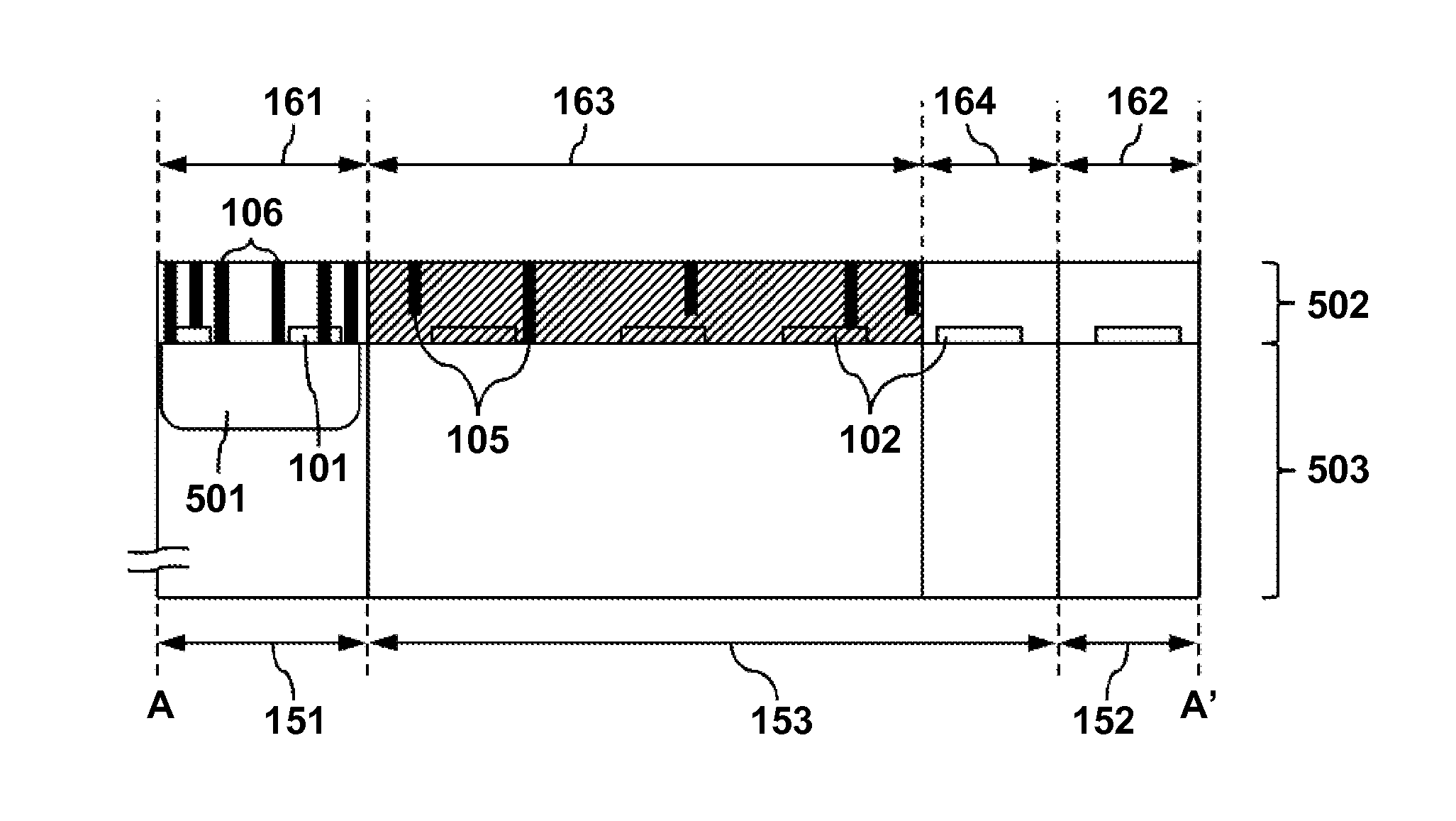
[0017]Detailed embodiments of a semiconductor device and a manufacturing method according to the present invention will now be described. Note that in the following explanation and drawings, the same reference numbers denote the same parts throughout a plurality of drawings. Hence, the same parts will be described by cross-referring to the plurality of drawings, and a description of the parts denoted by the same reference numerals will appropriately be omitted.

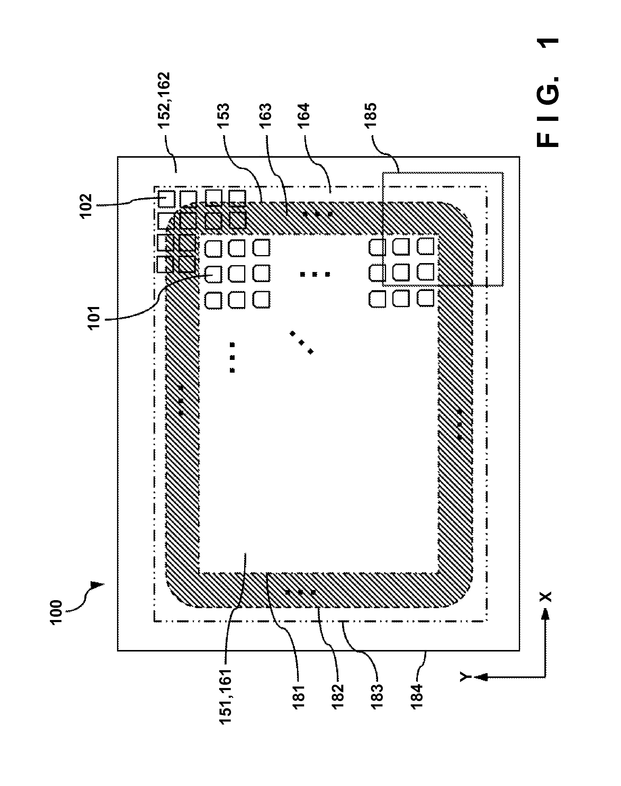
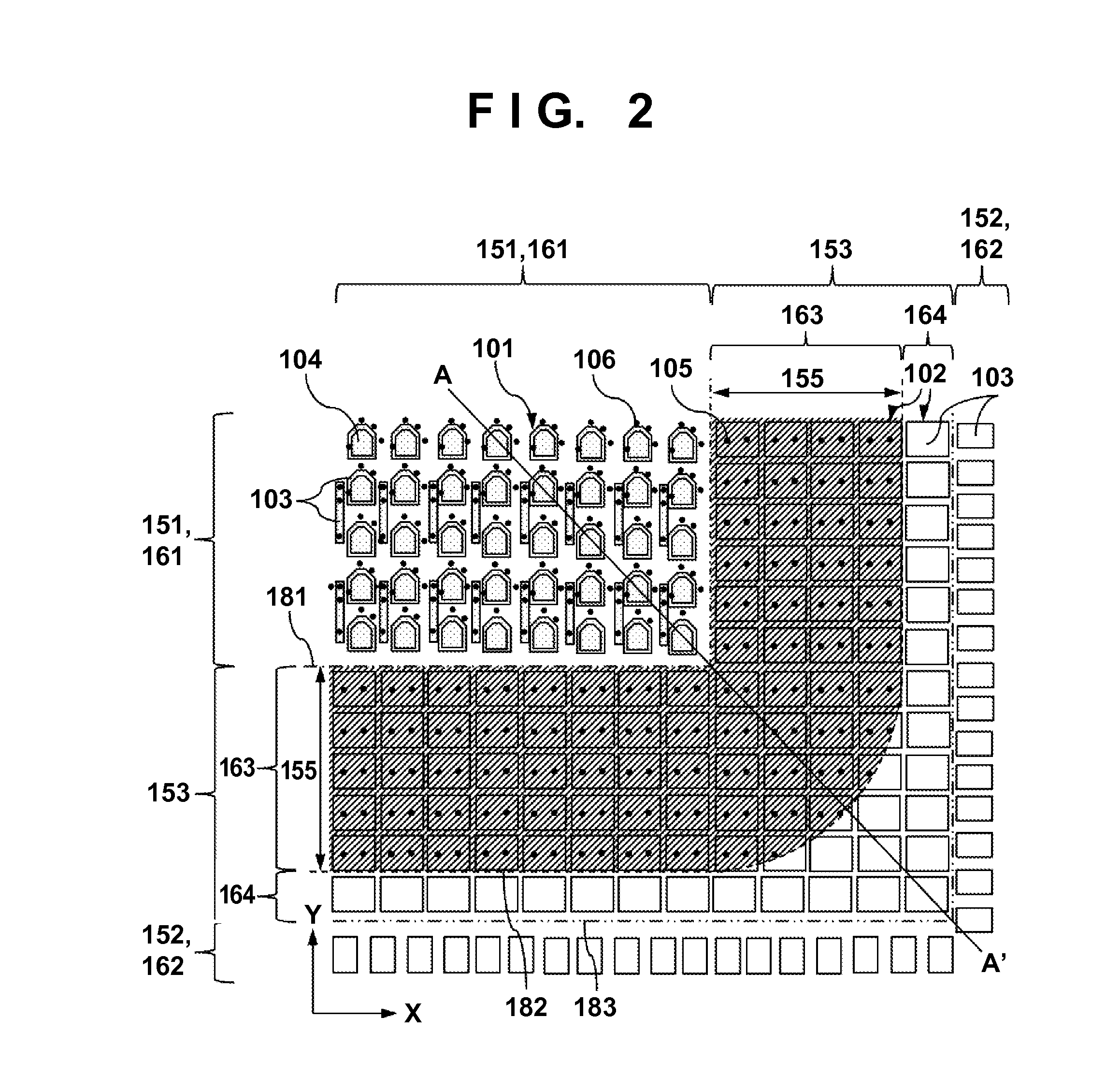
[0018]The structure and manufacturing method of the semiconductor device according to the present invention will be described with reference to FIGS. 1 to 4, 5A, and 5B. In this embodiment, the semiconductor device includes a cell area in which unit circuits are arranged in a matrix. As an example of the semiconductor device, a solid-state image sensor including a pixel area serving as a cell area where pixel circuits that are unit circuits are arranged periodically, and a peripheral area arranged around the pixel area will be...


PUM


Abstract

A semiconductor device is provided. The device includes a substrate with a cell and a peripheral area, and an insulating layer. The insulating layer comprises a first region located on the cell area and having outer edge along the cell area, a second region located on the peripheral area and having inner edge along the cell area, a third region located on an area between the cell and the peripheral area and a fourth region located between the second and the third region and forming a boundary with the third region. A conductive member is embedded in the first and the third region and no conductive member is embedded in the fourth region. The boundary has a curbed portion.

Description

BACKGROUND OF THE INVENTION[0001]1. Field of the Invention[0002]The present invention relates to a semiconductor device, a method of manufacturing the same, and a camera.[0003]2. Description of the Related Art[0004]Concerning planarization using chemical mechanical polishing (CMP), there is known a problem of a difference in polishing speed, which is caused by unevenness of the density of a pattern formed on a surface to be planarized. This may greatly lower the planarity. In particular, local overpolishing called Edge Over Erosion (EOE) occurs at the boundary between a region with a high pattern density and a region with a low pattern density.[0005]Japanese Patent Laid-Open No. 2006-100571 describes arranging dummy via hole plugs while gradually decreasing the dummy via hole plug density from a region where via hole plugs are formed.SUMMARY OF THE INVENTION[0006]In a conventional technique, a portion where suppression of EOE is insufficient may be generated. Some embodiments of the...

Claims


Application Information

Patent Timeline
IPC IPC(8): H01L21/768H04N5/225H01L23/528H01L21/321H01L27/146
CPCH01L21/76897H01L21/3212H04N5/2251H01L23/528H01L27/14636H01L27/14607H01L23/522H01L21/7684H01L27/14603H04N25/633
Inventor ITO, KEISUKE
Owner CANON KK
Why Eureka
Try Eureka