
Semiconductor device

a technology of semiconductor devices and semiconductors, applied in the direction of semiconductor devices, basic electric elements, electrical equipment, etc., can solve the problems of reducing the breakdown resistance of semiconductor devices, failure to take sufficient measures, and n-type emitter regions, so as to reduce reduce the number of n-type emitter regions, and reduce the effect of the number of emitter regions

Inactive Publication Date: 2016-05-19
TOYOTA JIDOSHA KK
View PDF36 Cites 3 Cited by
  • Summary
  • Abstract
  • Description
  • Claims
  • Application Information

AI Technical Summary

Benefits of technology

The patent describes a technology to improve the durability of semiconductor devices by reducing the number of electrons that flow from emitter regions and preventing them from concentrating on a specific area. This is achieved by configuring the emitter regions in a way that reduces the number of emitter regions in the middle inter-trench region and avoids contact with both first and second trenches. This reduces the likelihood of electrons flowing into the drift region and suppresses the concentration of currents, ultimately increasing the breakdown resistance of the semiconductor device. Additionally, the technology achieves a reduction in the on-resistance of the semiconductor device by preventing hole accumulation in the middle inter-trench region.

Problems solved by technology

The IGBT of Japanese Patent Application Publication No. 2013-150000 mainly aims to reduce the on-resistance and, as such, fails to take sufficient measures against a phenomenon in which an excessive number of electrons flows from the emitter regions into the drift region and the semiconductor device breaks down.
However, depending on the position where the narrowly-confined emitter regions are disposed, electrons can undesirably concentrate on a local region, thus causing a reduction in the breakdown resistance of the semiconductor device.

Method used


Image

  • Semiconductor device
  • Semiconductor device
  • Semiconductor device

Examples


first embodiment

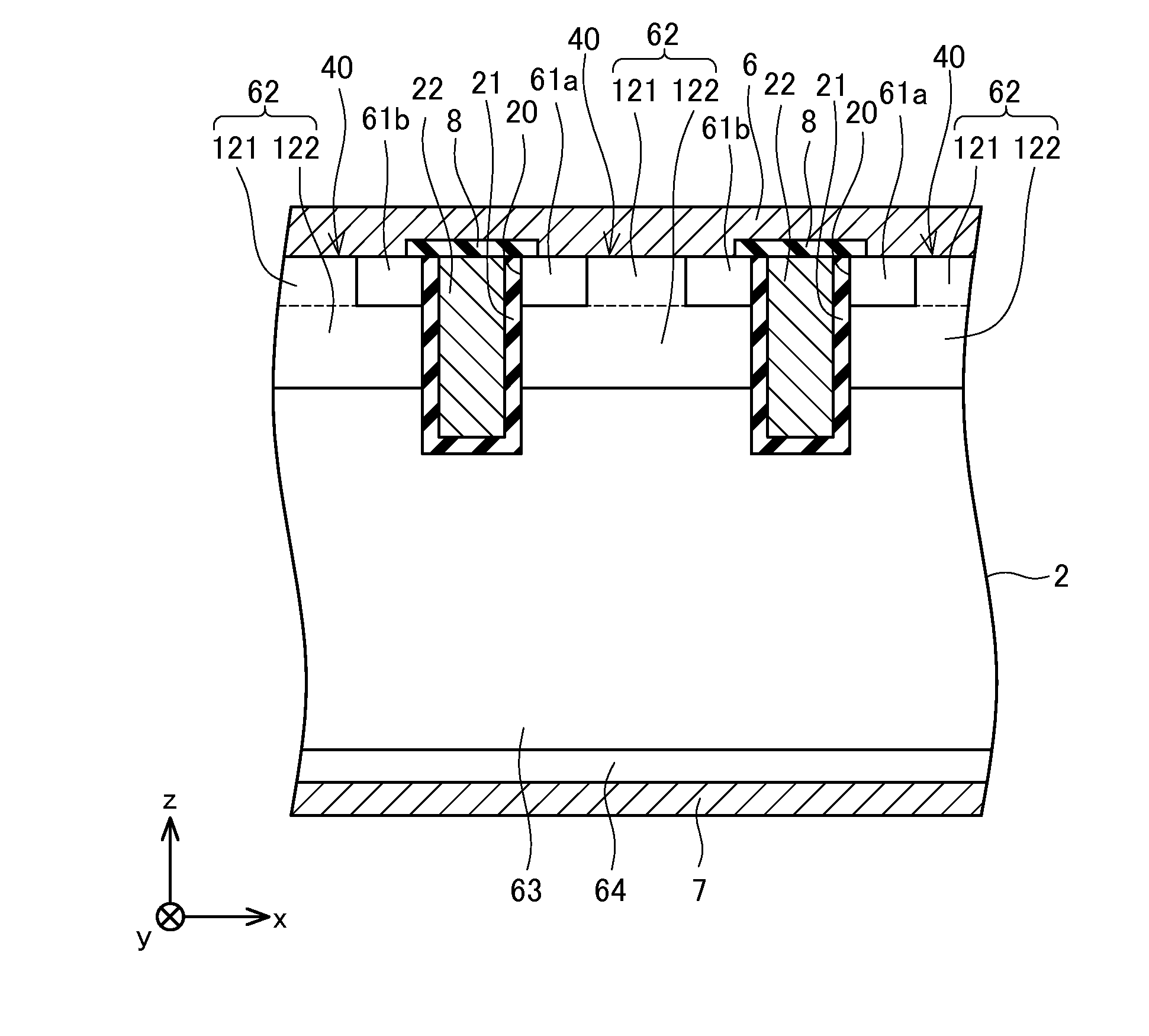
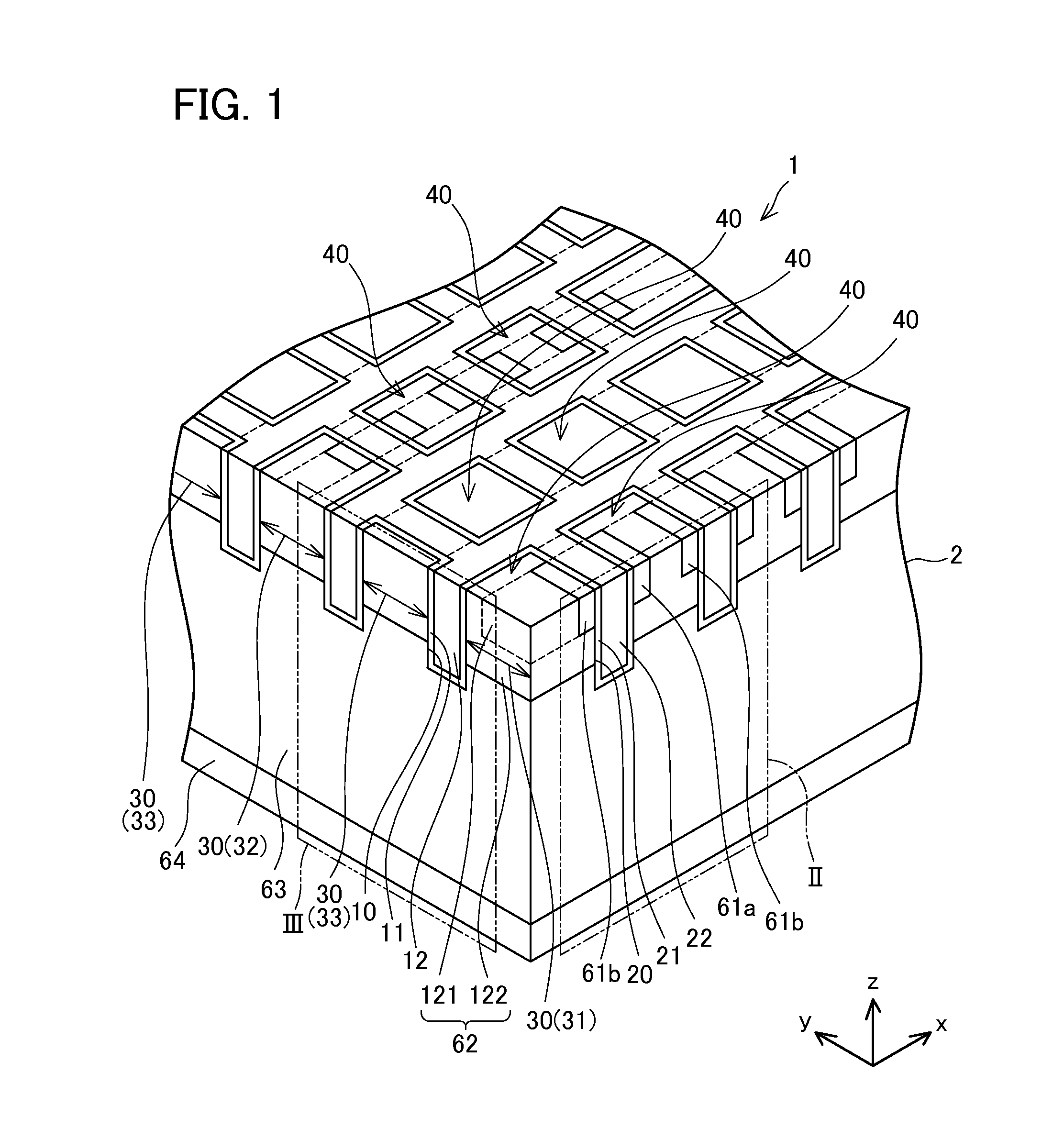
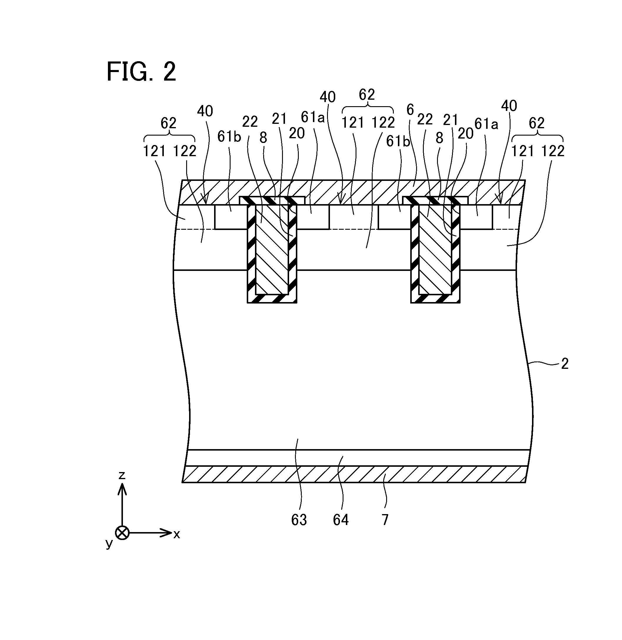
[0021]An embodiment will be described below with reference to the accompanying drawings. As shown in FIGS. 1 to 3, a semiconductor device 1 according to a first embodiment includes a semiconductor substrate 2, a front surface electrode 6, and a back surface electrode 7 (Note that, for the sake of viewability of the drawing, FIG. 1 omits to show the front surface electrode 6 and the back surface electrode 7.).

[0022]The semiconductor substrate 2 is made of silicon carbide (SiC). In another embodiment, the semiconductor substrate 2 may be made of silicon (Si), gallium nitride (GaN), or the like. A semiconductor element is disposed in the semiconductor substrate 2. The present embodiment takes an IGBT (insulated gate bipolar transistor) as an example of the semiconductor element.

[0023]The front surface electrode 6 and the back surface electrode 7 are made of a conductive metal such as aluminum (Al), copper (Cu), or the like. The front surface electrode 6 is disposed on a front surface o...

second embodiment

[0046]In the embodiment described above, a single middle inter-trench region 33 was disposed in between the first inter-trench region 31 and the second inter-trench region 32. However, the present disclosure may not be limited to this configuration. In a second embodiment, as shown in FIG. 6, a plurality of middle inter-trench regions 33 may be disposed between the first inter-trench region 31 and the second inter-trench region 32. At least one middle inter-trench region 33 should be disposed between the first inter-trench region 31 and the second inter-trench region 32. Such a configuration also makes it possible to, while suppressing local concentration of currents, suppress the number of electrons that are implanted.

third embodiment

[0047]In the embodiment described above, the second trenches 20 are disposed in the middle inter-trench region 33 interposed between the first inter-trench region 31 and the second inter-trench region 32. However, the present disclosure may not be limited to this configuration. In a third embodiment, as shown in FIG. 7, the second trenches 20 may not be disposed in a middle inter-trench region 33 interposed between the first inter-trench region 31 and the second inter-trench region 32. Such a configuration also makes it possible to, while suppressing local concentration of currents, suppress the number of electrons that are implanted.


PUM


Abstract

A semiconductor device has emitter regions disposed in at least one cell region in a first inter-trench region, not disposed in a middle inter-trench region, and disposed in at least one cell region in the second inter-trench region. Each of the emitter regions is disposed at a position that is not in contact with first trenches but is in contact with two second trenches defining the corresponding cell region.

Description

CROSS-REFERENCE TO RELATED APPLICATION[0001]This application claims priority to Japanese Patent Application No. 2014-232836 filed on Nov. 17, 2014, the contents of which are hereby incorporated by reference into the present application.TECHNICAL FIELD[0002]The present application relates to a semiconductor device.DESCRIPTION OF RELATED ART[0003]Japanese Patent Application Publication No. 2013-150000 discloses a semiconductor device fabricated in a semiconductor substrate. The semiconductor device is a vertical IGBT. The semiconductor device includes: a p-type body region disposed at one portion of the semiconductor substrate in a cross sectional view of the semiconductor substrate; an n-type drift region disposed below the body region in the cross sectional view; and n-type emitter regions separated from the drift region by the body region and exposed on an upper surface of the semiconductor substrate. The semiconductor device further includes: a trench extending from the upper surf...

Claims


Application Information

Patent Timeline
IPC IPC(8): H01L29/739H01L29/06H01L29/10
CPCH01L29/7397H01L29/0696H01L29/1095H01L29/0619H01L29/407
Inventor HIRABAYASHI, YASUHIROSENOO, MASARU
Owner TOYOTA JIDOSHA KK
Learn More