Method of manufacturing light emitting diode package structure

Inactive Publication Date: 2016-06-02
ACHROLUX
View PDF0 Cites 17 Cited by
  • Summary
  • Abstract
  • Description
  • Claims
  • Application Information

AI Technical Summary

Benefits of technology

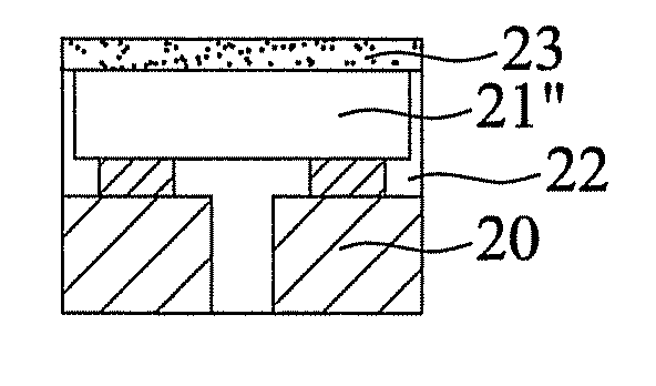
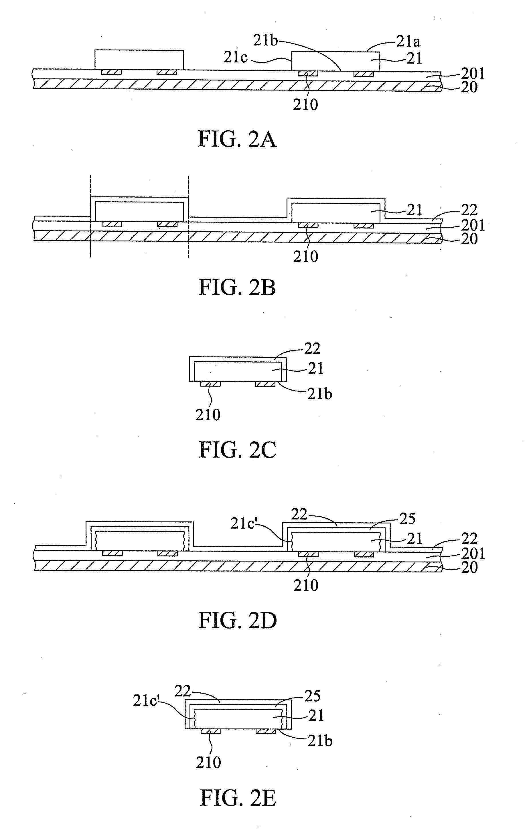
[0020]From the above, the method of manufacturing a light-emitting package structure according to the present invention disposes a light emitting element on a carrier by a chip scale package method. Then, a reflective film of extremely thin thickness is formed, such that the thickness and width of the package structure can be greatly reduced, so as to comply the demand of minimization.
[002

Problems solved by technology

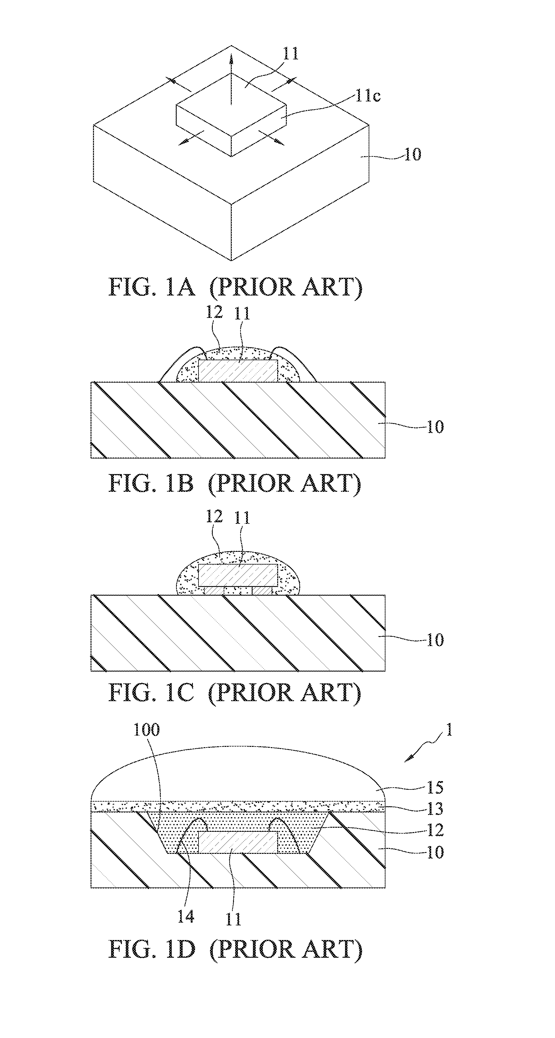
Although the conventional LED package 1 utilizes the reflective cup 100 and fluorescent layer 13 to allow the light emitting face of the LED package 1 face up to solve the problem of the significant variation of color temperature, the fluorescent

Method used


Image

  • Method of manufacturing light emitting diode package structure
  • Method of manufacturing light emitting diode package structure
  • Method of manufacturing light emitting diode package structure

Examples


Example

[0036]The following illustrative embodiments are provided to illustrate the disclosure of the present invention, these and other advantages and effects can be apparently understood by those in the art after reading the disclosure of this specification.

[0037]It should be advised that the structure, ratio, and size as illustrated in this context are only used for disclosures of this specification, provided for persons skilled in the art to understand and read, and technically do not have substantial meaning. Any modification of the structure, change of the ratio relation, or adjustment of the size should be involved in the scope of disclosures in this specification without influencing the producible efficacy and the achievable objective of this specification. Also, the referred terms such as “on”, “first”, “second” and “one” in this specification are only for the convenience to describe, not for limiting the scope of embodiment in the present invention. Those changes or adjustments of...


PUM


Abstract

A method of manufacturing a light-emitting package structure is provided. The method includes disposing at least one light emitting element on a carrier and forming a reflective material. The light emitting element has opposite first and second sides and a plurality of third sides connected to the first side and the second side. The light emitting element is disposed on the carrier via the second side. The reflective material is formed on the third side of the light emitting element, so as to form a reflective film.

Description

BACKGROUND OF THE INVENTION[0001]1. Field of the Invention[0002]The present invention relates to coating structures, and, more particularly, to a method of manufacturing a light emitting diode package structure.[0003]2. Description of Related Art[0004]With the booming development in the electronic industry, electronic products gradually become compact in form, and the research for the functionality pursuits for high performance, high functionality, and high processing speed. Light-emitting diodes (LEDs) are variously employed in electronic products that require lighting since the advantages of long lifecycle, small volume, high shock resistance, and low power consumption. Therefore, the application of LED becomes popular in industry, various electronic products, and appliances.[0005]As shown in FIG. 1A, typically when an LED element 11 is disposed on a substrate 10, an upper surface and adjacent four (not limited to four) side surfaces 11c of the LED element 11 are all light emittin...

Claims


Application Information

Patent Timeline
IPC IPC(8): H01L33/60H01L33/62H01L33/50
CPCH01L33/60H01L33/502H01L33/62H01L2933/0033H01L2933/0041H01L2933/0066H01L2933/0058H01L33/0095H01L33/46H01L33/56H01L2933/005H01L2224/48091H01L2224/8592H01L2924/00014
Inventor LING, PEICHINGLIU, DEZHONG
Owner ACHROLUX
Why Eureka
Try Eureka