

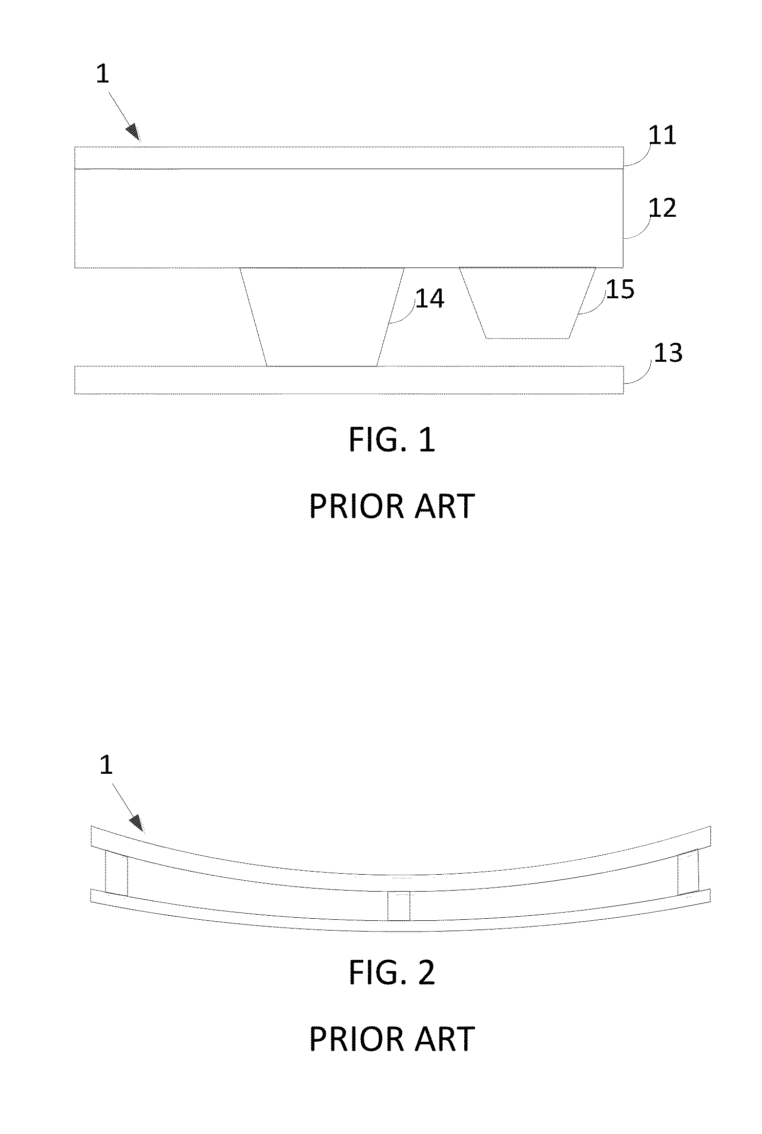
Curved liquid crystal display panel and manufacturing method thereof
- Summary
- Abstract
- Description
- Claims
- Application Information
AI Technical Summary
Benefits of technology
Problems solved by technology
Method used
Image

Examples
first embodiment
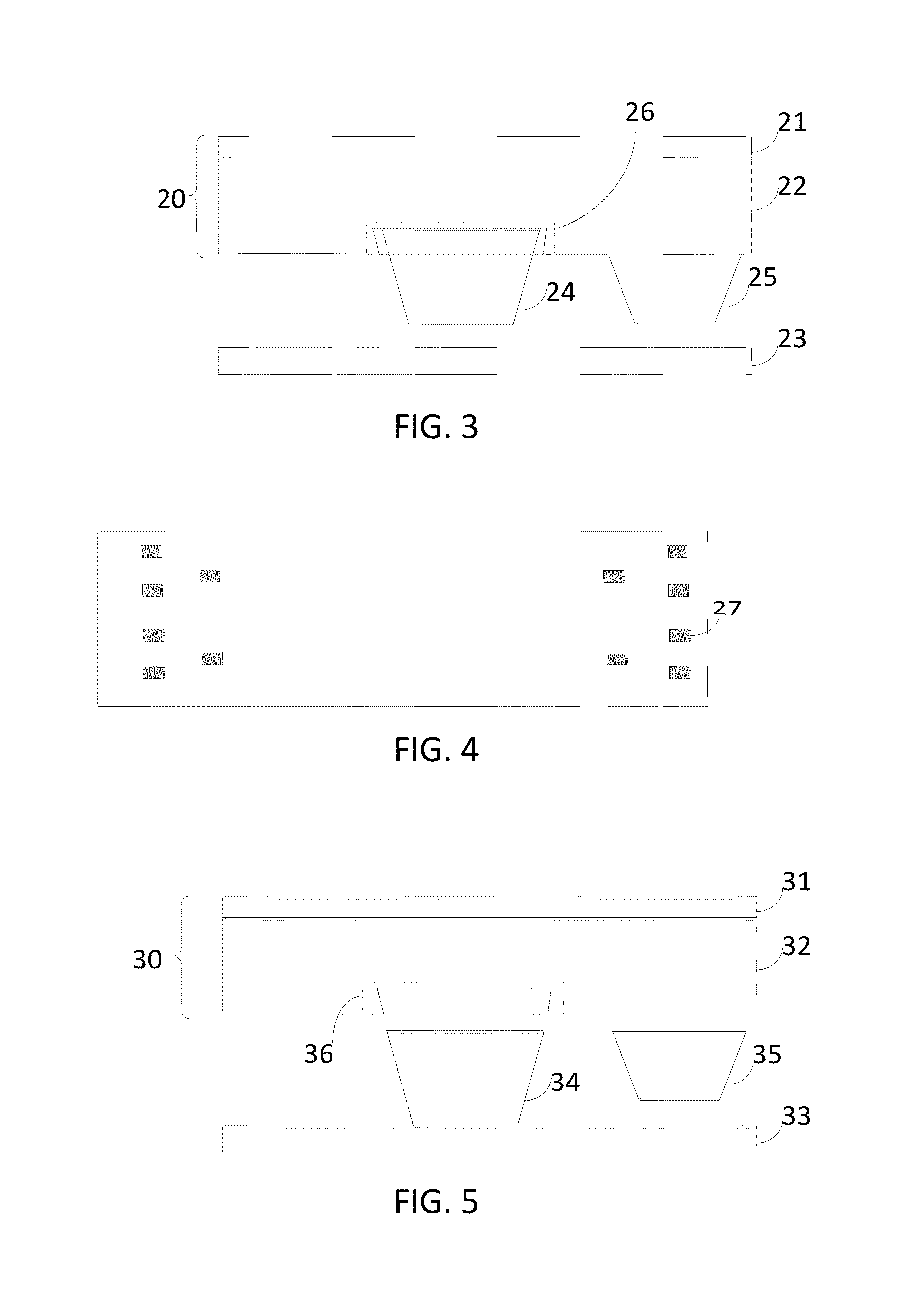
[0049]With reference to FIG. 3, FIG. 3 is a schematic view of a partial structure of a curved liquid crystal display panel according to the present invention.
[0050]The curved liquid crystal display panel of the present invention comprises a first substrate, a second substrate, a liquid crystal layer, a plurality of photo spacers. The first substrate may be a color-filter substrate 20. The second substrate may be an array substrate 23. The color-filter substrate 20 includes a substrate 21 and a color filter film 22. The liquid crystal layer is mounted between the first substrate and the second substrate. The photo spacers are used for maintaining a gap between the first substrate and the second substrate. The photo spacers are divided into a plurality of primary photo spacers 24 and a plurality of secondary photo spacers 25. A color-filter photoresist layer having at least one concave portion 26 is formed on the color-filter substrate 20. The concave portion 26 of the color-filter ph...
second embodiment
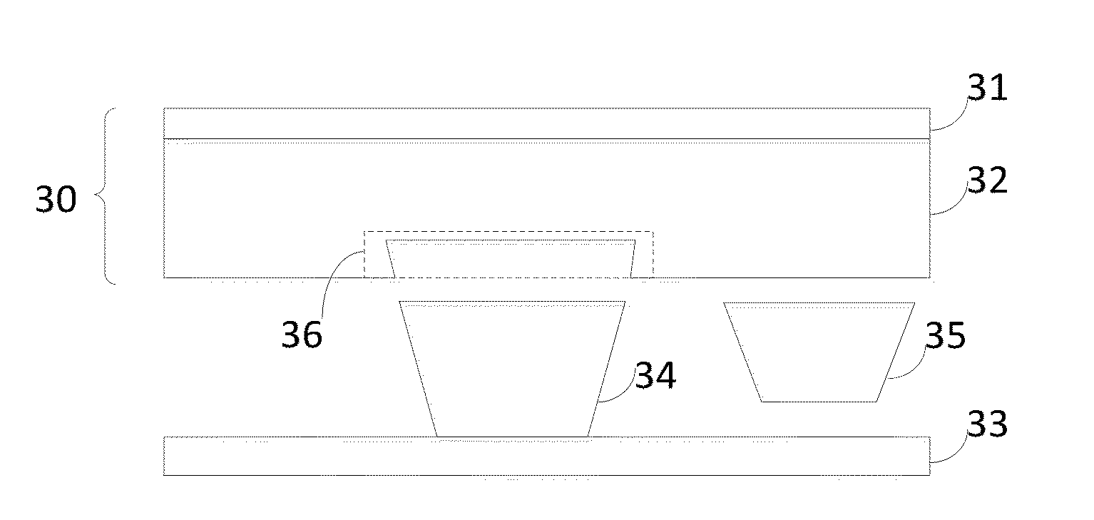
[0060]With further reference to FIG. 5, FIG. 5 is a schematic view of a partial structure of a curved liquid crystal display panel according to the present invention.
[0061]The curved liquid crystal display panel of the present invention comprises a first substrate, a second substrate, a liquid crystal layer, a plurality of photo spacers. The first substrate may be a color-filter substrate 30. The second substrate may be an array substrate 33. The color-filter substrate 30 includes a substrate 31 and a color filter film 32. The liquid crystal layer is mounted between the first substrate and the second substrate. The photo spacers are used for maintaining a gap between the first substrate and the second substrate. The photo spacers are divided into a plurality of primary photo spacers 34 and a plurality of secondary photo spacers 35. A color-filter photoresist layer having at least one concave portion 36 is formed on the color-filter substrate 30. The concave portion of the color-filt...
third embodiment
[0065]With further reference to FIG. 6, FIG. 6 is a schematic view of a partial structure of a curved liquid crystal display panel according to the present invention.
[0066]The curved liquid crystal display panel of the present invention comprises a first substrate, a second substrate, a liquid crystal layer and a plurality of photo spacers. The liquid crystal layer is mounted between the first substrate and the second substrate. The first substrate may be a COA (short for color filter on array) substrate 40. A plurality of thin-film transistors, data lines, scanning lines and pixel electrodes are all formed on the same layer such as an array driving layer 41. The COA substrate is to combine the color filter film 42 with the array driving layer 41 on the same substrate, such as the first substrate. In general, the color filter film 42 is mounted upon the array driving layer 41, wherein the second substrate is provided with a common electrode so that each of the pixel electrodes on th...
PUM
 Abstract
Description
Claims
Application Information