Capacitive touch panel with single sensing layer

a capacitive touch and sensing layer technology, applied in the field of capacitive touch panels with single sensing layer, can solve the problems of increasing packaging cost and volume of ic, and achieve the effects of reducing volume and manufacturing cost of ic, reducing the amount of contacts, and reducing the volume of i

Inactive Publication Date: 2016-06-16
ELAN MICROELECTRONICS CORPORATION
View PDF1 Cites 5 Cited by
  • Summary
  • Abstract
  • Description
  • Claims
  • Application Information

AI Technical Summary

Benefits of technology

[0008]An objective of the present invention is to provide a capacitive touch panel with single sensing layer reduces the amount of the contacts to decrease the volume and the manufacturing cost of the IC without increasing areas and losing resolution.

Problems solved by technology

When the leads are increased, the packaging cost and the volume of the IC is also increased.

Method used


Image

  • Capacitive touch panel with single sensing layer
  • Capacitive touch panel with single sensing layer
  • Capacitive touch panel with single sensing layer

Examples


Embodiment Construction

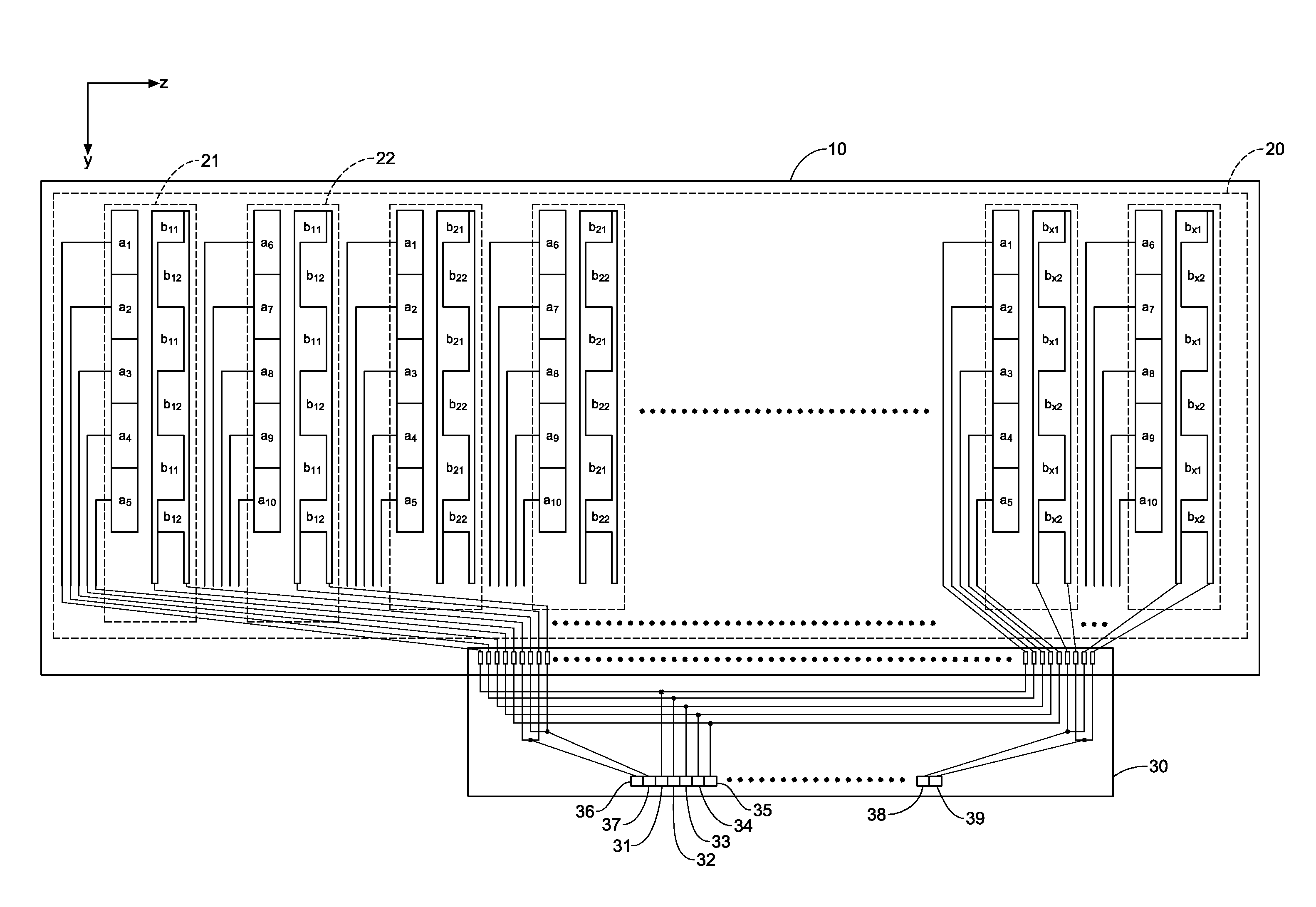
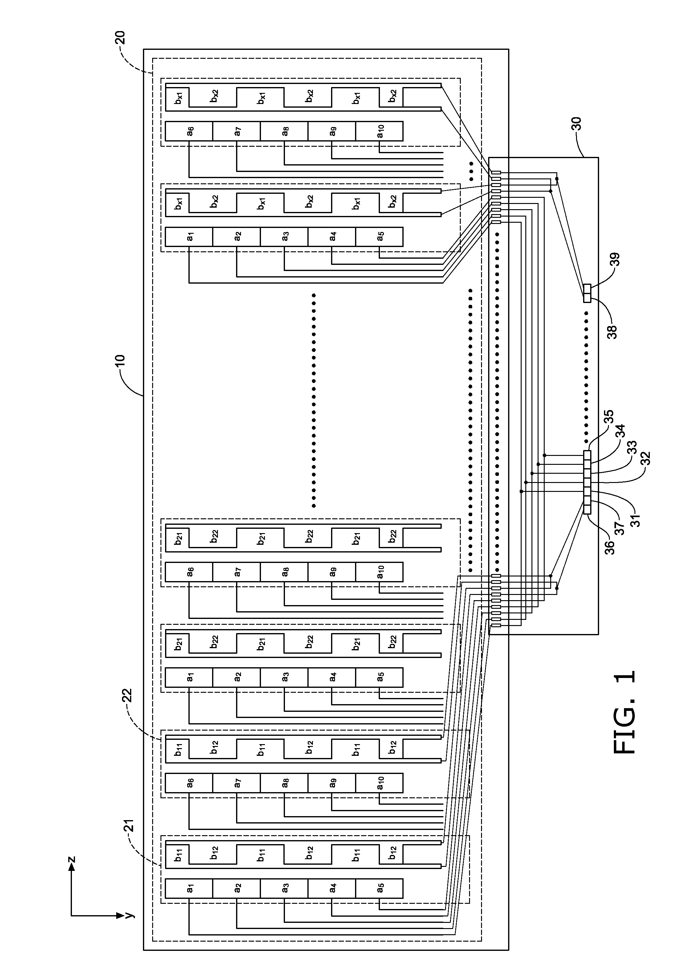
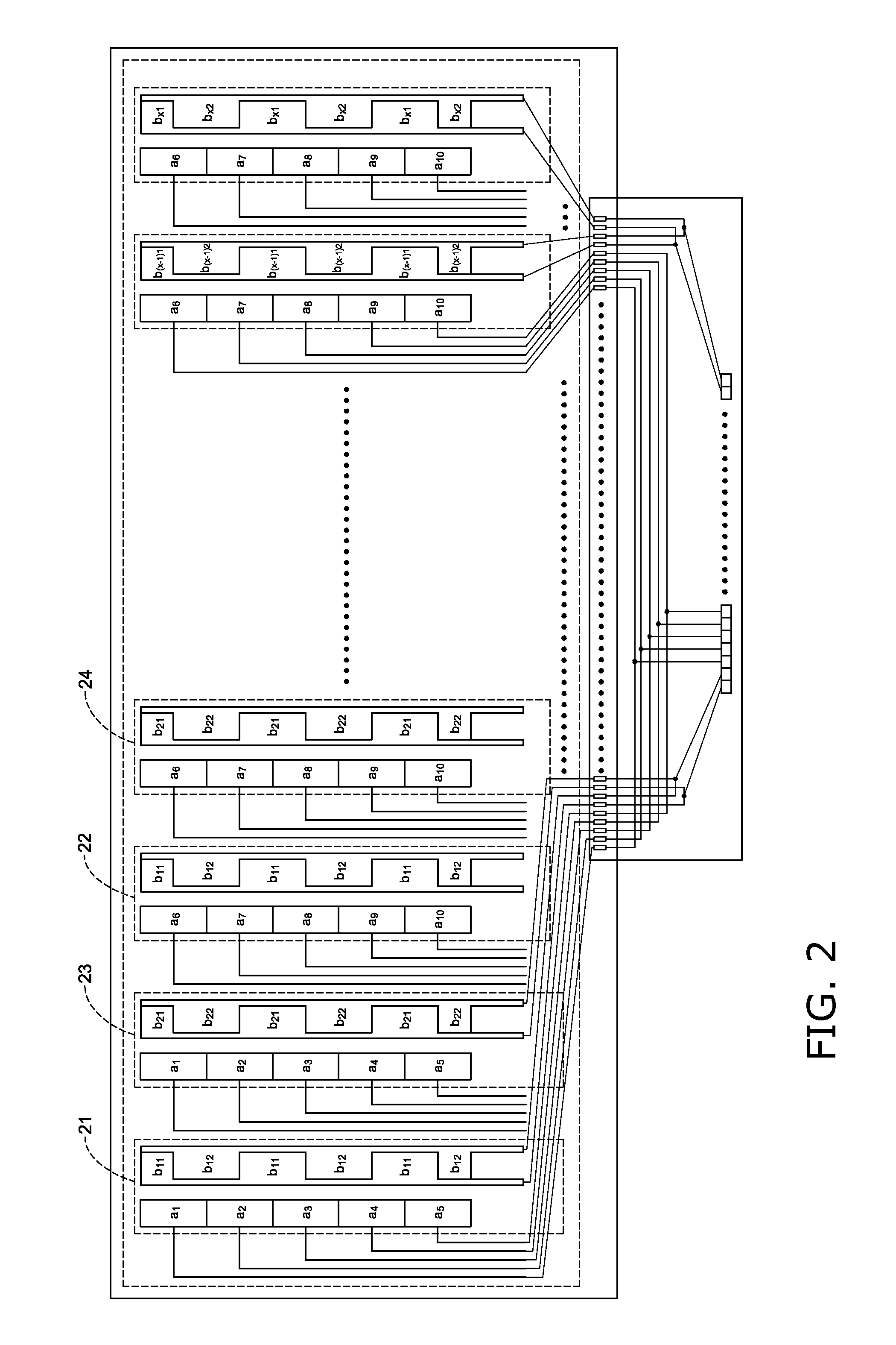
[0045]With reference to FIG. 1 a capacitive touch panel with single sensing layer in accordance with the present invention comprises a substrate 10 and a sensing layer 20. The sensing layer 20 is formed on one side surface of the substrate 10. The sensing layer 20 comprises n electrode sets. The electrode sets may be parallel to each other. The x-th electrode set comprises i a-th electrodes and multiple bx-th electrodes. The a-th electrodes include an a1-th electrode, an a2-th electrode . . . , to an ai-th electrode. The bx-th electrodes include multiple bx1-th electrodes, multiple bx2-th electrodes . . . , to multiple bxj-th electrodes. For example, the first electrode set shown in FIG. 1 has the a-th electrodes including an a1-th electrode, an a2-th electrode . . . to an a10-th electrode and the bx-th electrodes including multiple b11-th electrodes and multiple b12-th electrodes.

[0046]Each electrode set comprises multiple electrode groups. Each electrode group has an a-th electrod...


PUM


Abstract

A capacitive touch panel with single sensing layer has a substrate. The substrate has the single sensing layer formed thereon. The sensing layer has multiple electrode sets. Each electrode set has multiple driving electrode rows and multiple receiving electrode rows arranged alternately. The multiple driving electrode rows of one electrode set have different driving electrodes, but different electrode sets have the same multiple driving electrode rows. The multiple receiving electrode rows of one electrode set are consisted of multiple same receiving electrodes, but different electrode sets have different receiving electrode rows. Therefore, using less contacts can also maintained the area and the solution so that the pins on the IC are also decreased. Thus, the volume of the IC is reduced and the packaging cost is also reduced.

Description

CROSS-REFERENCE TO RELATED APPLICATIONS[0001]This application is based upon and claims priority under 35 U.S.C. 119 from Taiwan Patent Application No. 103143272 filed on Dec. 11, 2014, which is hereby specifically incorporated herein by this reference thereto.BACKGROUND OF THE INVENTION[0002]1. Field of the Invention[0003]The present invention relates to a capacitive touch panel with single sensing layer, especially to a touch panel as an input device for an electronic device.[0004]2. Description of the Prior Arts[0005]Capacitive touch panels with single sensing layer are widely used as input devices. With reference to FIG. 5, a conventional capacitive touch panel with single sensing layer has a sensing layer 40 mounted on one side of a substrate 50 and having multiple driving electrode rows and multiple receiving electrode rows alternately arranged along a first direction. The driving electrode rows and the receiving electrode rows are formed on the same surface. Each driving elect...

Claims


Application Information

Patent Timeline
Patent Type & Authority Applications(United States)
IPC IPC(8): G06F3/044G06F3/041
CPCG06F3/044G06F2203/04112G06F2203/04103G06F3/0416G06F1/22G06F3/04164G06F3/0443G06F3/0445
Inventor WU, CHIA-MUCHENG, TING-HSUAN
Owner ELAN MICROELECTRONICS CORPORATION
Why Eureka
Try Eureka