Organic light-emitting device and organic display apparatus

a light-emitting device and organic technology, applied in the direction of organic semiconductor devices, solid-state devices, thermoelectric devices, etc., can solve the problem of light emission efficiency declin

Active Publication Date: 2016-06-30
PANASONIC INTELLECTUAL PROPERTY MANAGEMENT CO LTD
View PDF16 Cites 6 Cited by
  • Summary
  • Abstract
  • Description
  • Claims
  • Application Information

AI Technical Summary

Benefits of technology

[0012]One non-limiting and exemplary embodiment provides an organic light-emitting device and an organic display apparatus capable of achieving securing of high visibility and inhibition of decline in contrast in a dark place, in a device structure where emitted light passes through a coating layer and is extracted outward, by inhibiting occurrence of a cloudy phenomenon even when external light enters, while inhibiting functional degradation of the organic layer under influence of substances such as water and oxygen that enter from outside, and outgas.
[0020]Therefore, the organic light-emitting device according to the above aspect is capable of achieving securing of high visibility and inhibition of decline in contrast in a dark place, in the device structure where emitted light passes through the coating layer and is extracted outward, by inhibiting occurrence of a cloudy phenomenon even when external light enters, while inhibiting functional degradation of the organic layer under influence of substances such as water and oxygen that enter from outside, and outgas.

Problems solved by technology

An organic layer included in a structure of the organic light-emitting device, such as an organic EL panel, is susceptible to entry of substances such as water and oxygen from outside, and to outgas (various kinds of gas including water and oxygen) emitted from components after the panel is completed.
This may produce a nonluminous region, such as a dark spot, and cause decline in light emission efficiency.

Method used


Image

  • Organic light-emitting device and organic display apparatus
  • Organic light-emitting device and organic display apparatus
  • Organic light-emitting device and organic display apparatus

Examples


first exemplary embodiment

1. Schematic Configuration of Organic EL Display Apparatus 1

[0084]A schematic configuration of organic EL display apparatus 1 according to a first exemplary embodiment of the present disclosure will be described with reference to FIG. 3 and FIG. 4.

[0085]As illustrated in FIG. 3, organic EL display apparatus 1 includes display panel 10 and drive-control circuit part 20 connected to display panel 10. Display panel 10 is an organic EL panel using electroluminescence of an organic material, and includes a plurality of pixels (picture elements).

[0086]As illustrated in FIG. 4, each of the pixels includes subpixel 10a that is a luminous part of red (R), subpixel 10b that is a luminous part of green (G), and subpixel 10c that is a luminous part of blue (B). In the present exemplary embodiment, the plurality of subpixels 10a to 10c are arranged in X-axis and Y-axis directions in a matrix (two-dimensional arrangement). Nonluminous region 10d is arranged between adjacent subpixels 10a to 10c. ...

second exemplary embodiment

[0187]A structure of display panel 30 according to a second exemplary embodiment of the present disclosure will be described with reference to FIG. 16. Note that, in FIG. 16, identical reference numerals are used to denote identical portions in the above first exemplary embodiment, and no further description will be made thereon.

[0188]As illustrated in FIG. 16, also in display panel 30 according to the present exemplary embodiment, EL panel part 11 and CP panel part 13 are joined by resin layer 35 disposed between EL panel part 11 and CP panel part 13. In display panel 30 according to the present exemplary embodiment, resin layer 35 is divided into two layers in a Z-axis direction. Specifically, resin layer 35 has a laminated structure of first resin element layer 351 disposed on a CP panel part 13 side (upper side of the Z-axis direction) and second resin element layer 350 disposed on an EL panel part 11 side (lower side of the Z-axis direction).

[0189]Between two layers 350, 351 th...

third exemplary embodiment

[0194]A structure of display panel 40 according to a third exemplary embodiment of the present disclosure will be described with reference to FIG. 17. Note that, in FIG. 17, identical reference numerals are used to denote identical portions in the above first exemplary embodiment, and no further description will be made thereon.

[0195]As illustrated in FIG. 17, also in display panel 40 according to the present exemplary embodiment, resin layer 45 disposed between EL panel part 11 and CP panel part 13 has a laminated structure of first resin element layer 451 and second resin element layer 450.

[0196]The present exemplary embodiment differs from the above second exemplary embodiment in that a surface on a light-emitting side of second resin element layer 450 (upper side of a Z-axis direction) has an uneven structure where protrusion 450a and recess 450b continue. This surface of second resin element layer 450 having periodic the uneven structure is called a photonic crystal (PC) struct...


PUM


Abstract

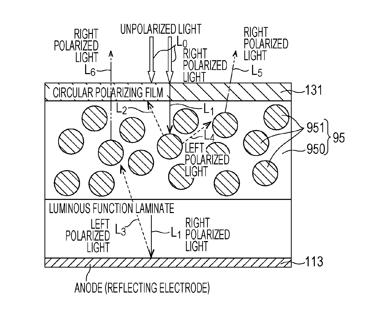
A display panel includes an EL panel part, a CP panel part, and a resin layer. Light is extracted from a luminous part including an organic luminous layer in the EL panel part in a direction of an arrow. The CP panel part includes a circular polarizing film. The resin layer is formed to cover an upper surface of the EL panel part, has a layer thickness of 15 μm, and includes a resin part and a plurality of getter particles dispersed in the resin part. The getter particles are dispersed at a density at which the getter particles do not overlap one another in plan view.

Description

BACKGROUND[0001]1. Technical Field[0002]The present disclosure relates to an organic light-emitting device and an organic display apparatus, and in particular to a structure of a resin layer disposed to cover a luminous part.[0003]2. Description of the Related Art[0004]In recent years, organic light-emitting devices, such as an organic EL (electro-luminescence) panel and organic EL lighting, have been intensively developed.[0005]An organic EL panel includes a first panel part in which an EL luminous part is formed and a second panel part disposed so as to face the first panel part with a gap between the first panel part and the second panel part. The first panel part and the second panel part are joined by a resin layer inserted between the first panel part and the second panel part.[0006]The first panel part has a structure including a TFT layer, a flat layer (insulating layer), an electrode, an organic luminous function layer, and an electrode laminated in this order on a substrat...

Claims


Application Information

Patent Timeline
Patent Type & Authority Applications(United States)
IPC IPC(8): H01L51/52H01L27/32
CPCH01L51/5259H01L51/5253H01L51/5275H01L51/5293H01L2251/558H01L27/3244H01L2251/301H01L2251/303H01L51/5268H10K59/122H10K50/846H10K50/854H10K50/8426H10K50/858H10K50/86H10K2102/3026H10K2102/351
Inventor MASUDA, HIROYUKI
Owner PANASONIC INTELLECTUAL PROPERTY MANAGEMENT CO LTD
Why Eureka
Try Eureka