Estimation of lifetime remaining for a consumable-part in a semiconductor manufacturing chamber

US20160216185A1Active Publication Date: 2016-07-28LAM RES CORP

Image

  • Estimation of lifetime remaining for a consumable-part in a semiconductor manufacturing chamber
  • Estimation of lifetime remaining for a consumable-part in a semiconductor manufacturing chamber
  • Estimation of lifetime remaining for a consumable-part in a semiconductor manufacturing chamber

Examples


Embodiment Construction

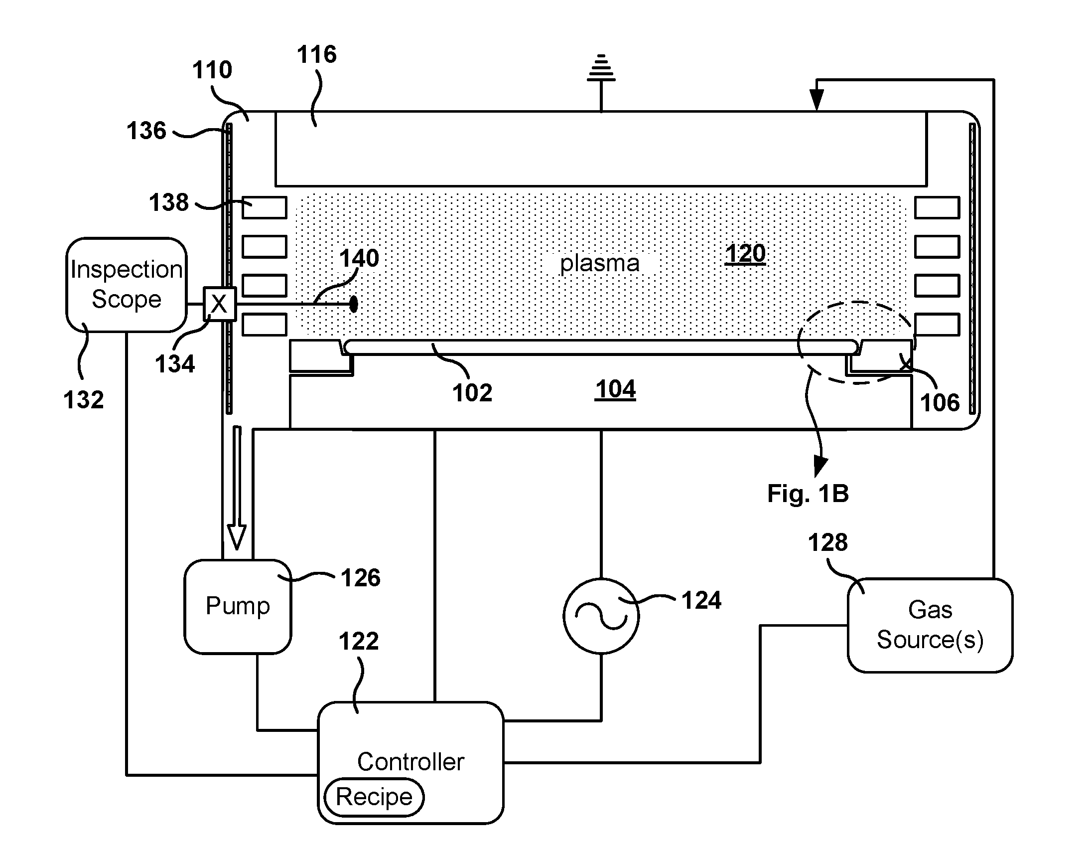
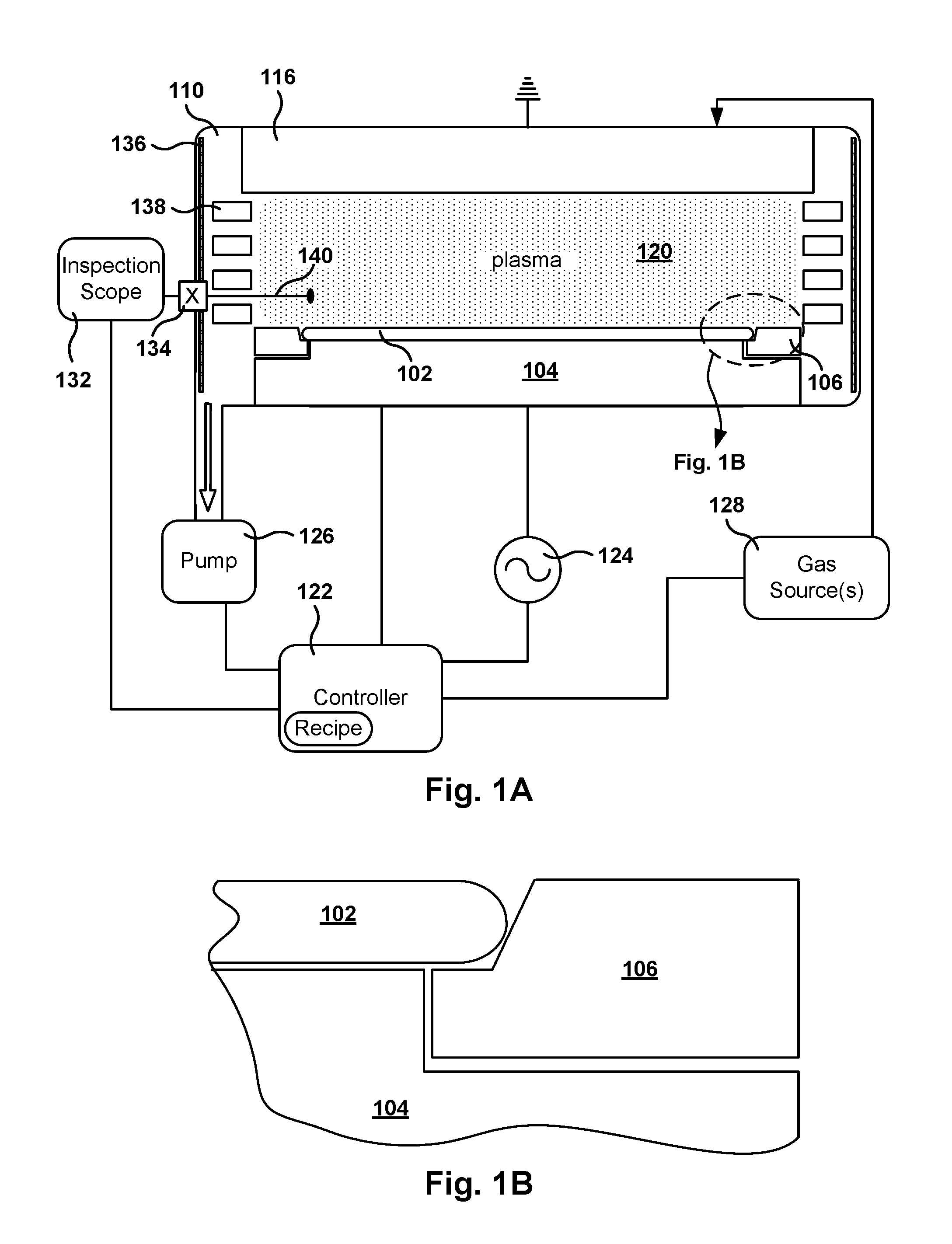
[0031]The following embodiments describe methods, devices, systems, and computer programs for generating system notifications regarding the lifetime remaining for consumable parts in a semiconductor processing chamber.

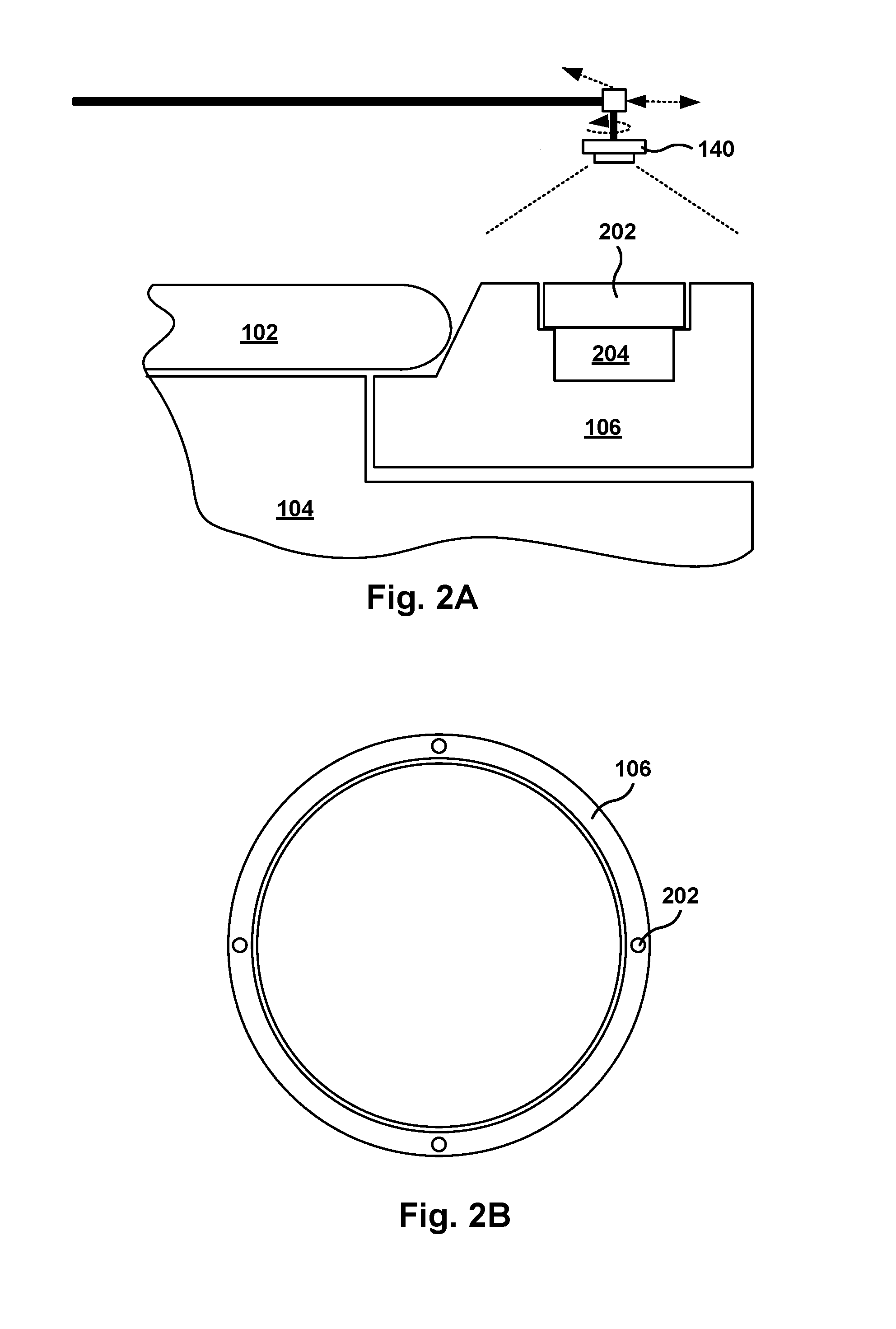
[0032]A trigger feature is embedded into the surface of a consumable part to assess the lifetime remaining of the part, such as an edge ring in a semiconductor chamber. In one implementation, the trigger feature includes a capping element above a space embedded into the edge ring. The capping element is coplanar with the edge ring, and as the top surface of the edge ring gets eroded due to etching on the chamber, the capping element is also eroded. After a certain amount of erosion, the capping element is completely worn off and the space underneath the capping element is exposed on the top surface of the edge ring. Visual inspection can then be used to analyze the surface of the edge ring and determine if the trigger feature is visible. Once the trigger feature is vis...


PUM

PropertyMeasurementUnit
Fractionaaaaaaaaaa
Fractionaaaaaaaaaa
Timeaaaaaaaaaa

Abstract

A consumable part, for use inside a chamber where plasma is used to process a semiconductor substrate, includes a body and a trigger feature. The body has a surface configured to be exposed to the plasma during processing in the chamber, and the trigger feature is integrated within the body. The trigger feature includes a void disposed under the surface of the body, where the void is configured to become visible when the surface is eroded from exposure to the plasma over time. The void becoming visible is an identifiable feature on the surface of the body that indicates a wear level for the consumable part, the wear level being associated with an amount of processing time remaining for the consumable part.

Description

CLAIM OF PRIORITY[0001]This application claims priority from U.S. Provisional Patent Application No. 62 / 109,016, filed Jan. 28, 2015, and entitled “ESTIMATION OF LIFETIME REMAINING FOR A CONSUMABLE-PART IN A SEMICONDUCTOR MANUFACTURING CHAMBER.” This provisional application is herein incorporated by reference.BACKGROUND[0002]1. Field of the Invention[0003]The present embodiments relate to methods for improving semiconductor process uniformity, and more particularly, methods, systems, and computer programs for generating system notifications regarding the lifetime remaining for consumable parts in a semiconductor processing chamber.[0004]2. Description of the Related Art[0005]Plasma has long been employed to process substrates (e.g., wafers or flat panels) to form electronic products (e.g., integrated circuits or flat panel displays). Semiconductor wafers are typically placed in an etch chamber with a photoresist mask layer to direct the etch of the underlying materials. The etching ...

Claims


Application Information

Patent Timeline
28 Jul 2016
Publication
US20160216185A1
IPC
G01N3/56; H01L21/67; C23C16/52; H01J37/32; C23C16/50
CPC
G01N3/56; H01J37/32009; H01J37/3244; H01L21/67253; C23C16/52; H01L21/67069; C23C16/50; H01J37/3299
Inventors
GOTTSCHO, RICHARD ALAN