Terahertz source chip, source device and source assembly, and manufacturing methods thereof

a technology of terahertz source and source device, which is applied in the direction of solid masers, semiconductor devices, electrical equipment, etc., can solve the problems of terahertz emission, low emission efficiency, low power, and finite mobility of two-dimensional electron gas, so as to achieve the effect of widening the operation temperature range and the emission frequency band

Inactive Publication Date: 2016-08-11
SUZHOU INST OF NANO TECH & NANO BIONICS CHINESE ACEDEMY OF SCI
View PDF2 Cites 12 Cited by
  • Summary
  • Abstract
  • Description
  • Claims
  • Application Information

AI Technical Summary

Benefits of technology

[0106]In the present invention, a plasmon polariton mode is formed by strongly coupling a terahertz wave mode within the terahertz resonant cavity with a plasma wave mode in the electron gas below the grating, and the terahertz wave can be generated by electrical excitation of the plasmon polariton. In

Problems solved by technology

However, the generation of the terahertz emission by this method always has problems of low emission efficiency, low power, and demand of low temperature.
However, the mobility of the two-dimensional electron gas is finite.
The

Method used


Image

  • Terahertz source chip, source device and source assembly, and manufacturing methods thereof
  • Terahertz source chip, source device and source assembly, and manufacturing methods thereof
  • Terahertz source chip, source device and source assembly, and manufacturing methods thereof

Examples


Embodiment Construction

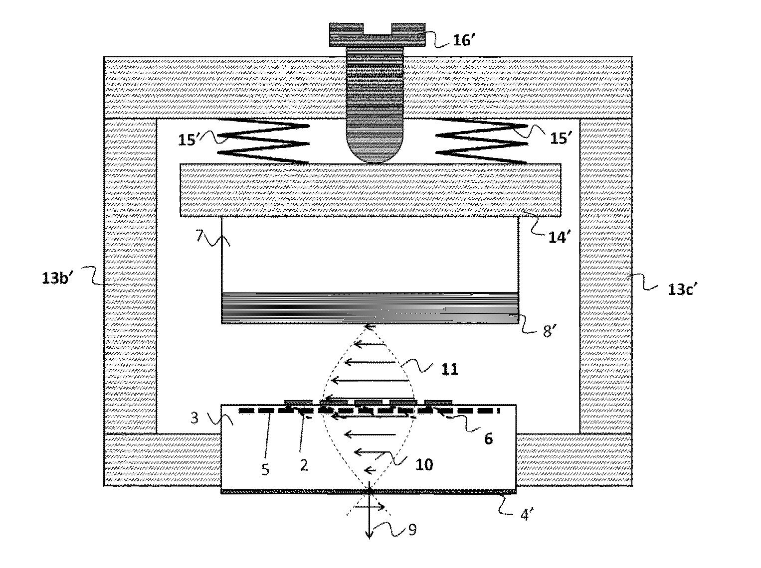
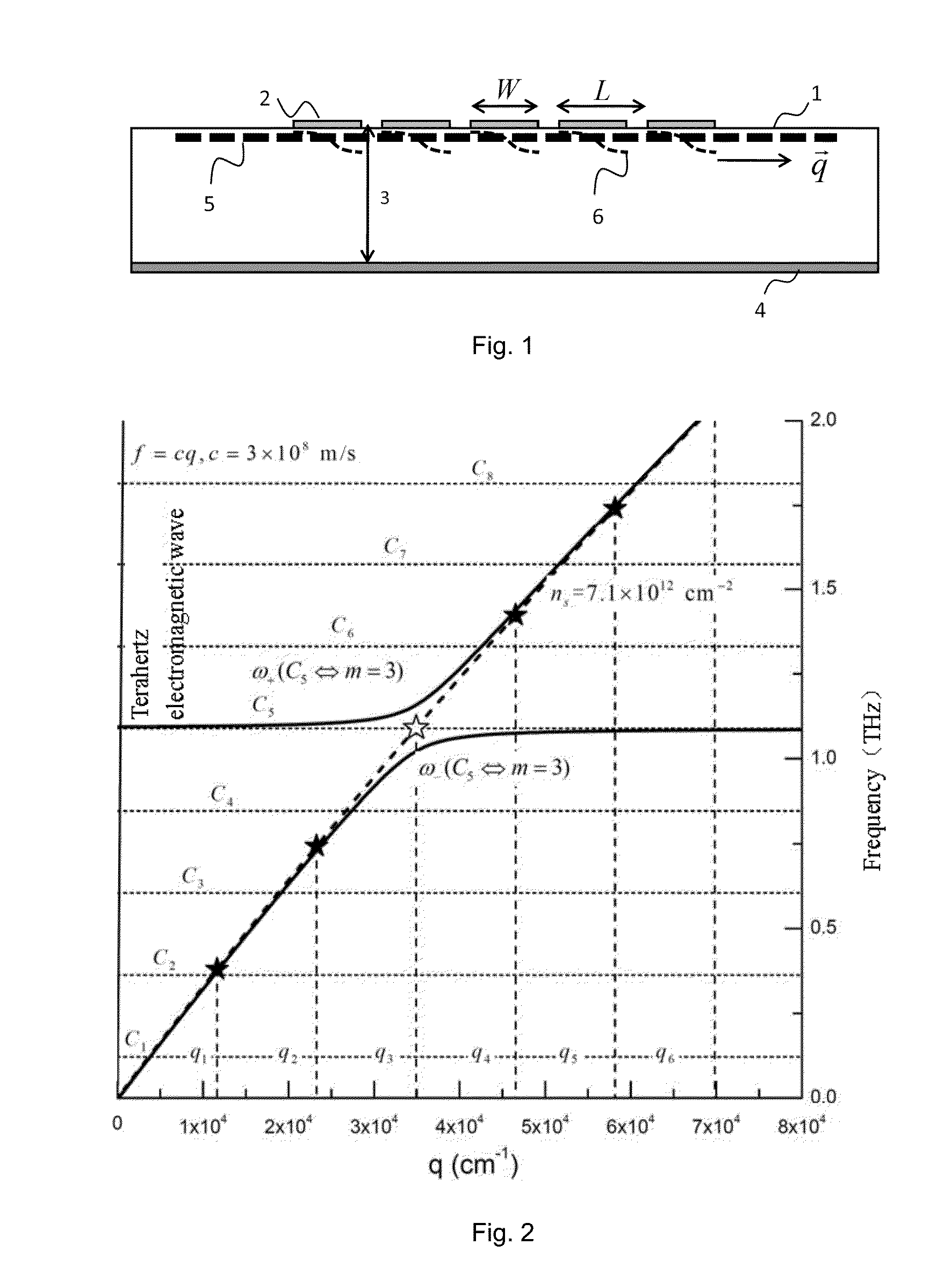
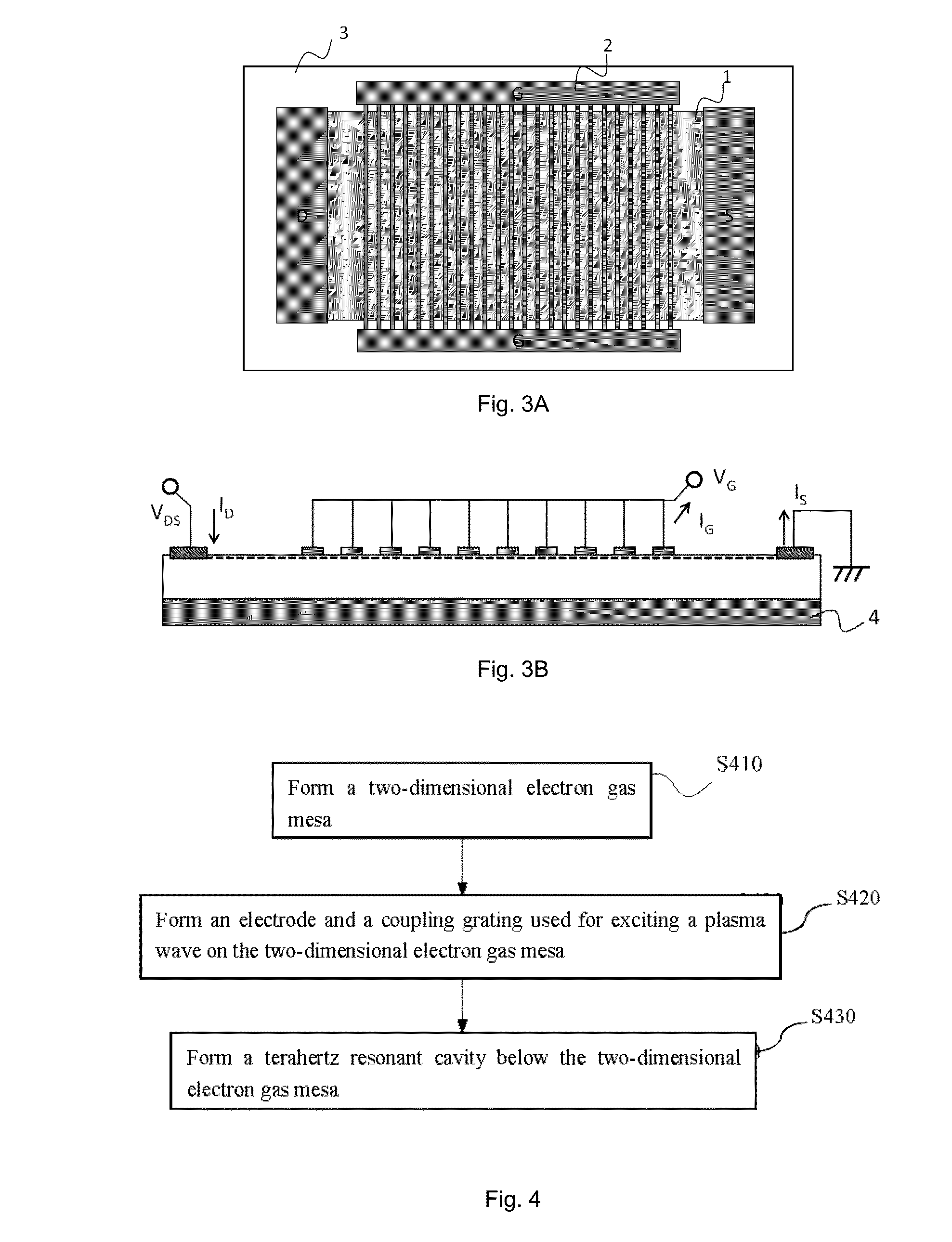
[0127]In implementations of the present invention, a terahertz source is realized by forming a plasmon polariton mode by strongly coupling a plasma wave mode with a cavity mode of a terahertz resonant cavity using a terahertz coupling grating. More specifically, a plasmon plaritron mode is formed by exciting a plasma wave in an electron gas by DC or AC voltage applied onto one or more electrodes of a terahertz source chip and strongly coupling the plasma wave mode with a terahertz wave mode in the resonant cavity using a grating, i.e., a new state having characteristics of both the plasma wave and the terahertz electromagnetic wave. Thus, the overall efficiency of conversion from the plasma wave to the terahertz radiation is improved. That is to say, in the present invention, by injecting DC or AC current into an electron gas to excite a plasma wave, the terahertz wave is generated since the grating and the terahertz resonant cavity strongly couple the plasma wave mode with the cavi...


PUM


Abstract

The present invention provides a terahertz source chip, a source device, a source assembly and manufacturing methods thereof. The source chip comprises: a two-dimensional electron gas mesa; an electrode formed on the two-dimensional electron gas mesa for exciting a plasma wave; a terahertz resonant cavity formed below the two-dimensional electron gas mesa, the terahertz resonant cavity having a total reflector on a bottom surface thereof; and a grating formed on the two-dimensional electron gas mesa for coupling a plasma wave pattern with a cavity mode of the terahertz resonant cavity to generate terahertz radiation. In the present invention, a plasmon polariton is formed by strongly coupling the cavity mode of the terahertz resonant cavity with the plasma wave mode in the two-dimensional electron gas below the grating, and the terahertz wave emission is realized by electrical excitation of the plasmon polariton. In this way, a problem of low frequency or low operating temperature caused by generating the terahertz emission based on high-frequency oscillation of a single electron or quantum transition of a single electron is avoided, and the emission frequency band and the operating temperature range are widened.

Description

TECHNICAL FIELD OF THE INVENTION[0001]The present invention relates to the technology for generating terahertz radiation, and in more particular to a terahertz source chip, a source device and a source assembly, and manufacturing methods thereof.BACKGROUND OF THE INVENTION[0002]Terahertz wave, as an electromagnetic wave having a band from 0.1 THz to 10 THz (1 THz=1000 GHz=1012 Hz) and a wavelength from 30 μm to −3 mm, is between millimeter wave and infrared light, which is also known as sub-millimeter wave or far-infrared radiation. The radiation of the terahertz wave is also referred to as terahertz radiation. A device or an apparatus enabling to generate the terahertz radiation is referred to as a terahertz source or a terahertz emitter.[0003]The existing technical solutions for generating the terahertz radiation may be mainly divided into the following three types.[0004]The first type is an electronics technical solution where high-frequency electromagnetic wave radiation is gene...

Claims


Application Information

Patent Timeline
IPC IPC(8): H01L33/10H01L33/06H01L33/32H01L33/58H01L33/34H01L33/28H01L33/26H01L33/54H01L33/00H01L33/30
CPCH01S1/02H01L29/42316H01L33/58H01L29/778H01L33/34H01L33/32H01L33/26H01L33/28H01L33/54H01L33/105H01L33/06H01L33/0095H01L33/0041H01L33/30
Inventor QIN, HUASUN, JIANDONGHUANG, YONGDANZHENG, ZHONGXINWU, DONGMINCAI, YONGZHANG, BAOSHUN
Owner SUZHOU INST OF NANO TECH & NANO BIONICS CHINESE ACEDEMY OF SCI
Why Eureka
Try Eureka