Conductive film and method of manufacturing the same

a manufacturing method and technology of conductive film, applied in the field of liquid crystal display, can solve the problems of poor conductivity, poor conductivity and mechanical performance, and limited stability and reliability, and achieve the effects of improving electrical conductivity bridge capability, reducing manufacturing costs, and improving environmental protection

Inactive Publication Date: 2016-08-18
TCL CHINA STAR OPTOELECTRONICS TECH CO LTD
View PDF3 Cites 18 Cited by
  • Summary
  • Abstract
  • Description
  • Claims
  • Application Information

AI Technical Summary

Benefits of technology

[0006]One object of the present invention is to provide a method of manufacturing conductive film. By introducing functionalized molecular having polar groups onto the surface of the graphene, distribution of the functionalized graphene in the adhesive resin can be improved.
[0007]One object of the present invention is to further provide a conductive film. A part or all of the conductive particles are the functionalized graphene such that the conductive particles can be uniformly distributed in the produced conductive film, and the conductive film can have outstanding electrical conductivity, thermal conductivity and adhesion strength.
[0023]The beneficial effect of the present invention is that by functionalizing the surface of the graphene, the obtained functionalized graphene can be uniformly distributed in the adhesive resin such that a better electrical conducting bridge capability can be obtained in the method of manufacturing the conductive film and the conductive film itself of the present invention. Compared to the conventional method of manufacturing conductive film, raw materials can be obtained more easily and economical, and is more environment friendly by using the functionalized graphene or mixture of the functionalized graphene and other conductive particles. Applying ultrasonic processing at the same time during the manufacturing procedure, the distribution and uniformity of the conductive particles can be improved and is beneficial on improving conductivity. In the conductive film of the present invention, a part or all of the conductive particles are the functionalized graphene such that the conductive particles can be uniformly distributed in the produced conductive film, and therefore the conductive film can have outstanding electrical conductivity, thermal conductivity and adhesion strength.

Problems solved by technology

Cu, Al and Ni are cheap and with good conductivity, however, they are easily to be oxidized in the air when the temperature is high such that the conductivity becomes poor and the stability and reliability is limited.
However, the golden ball has the following defects: (1) the interface force between the plastic layer and the metal layer is poor so that the conductivity and mechanical performance becomes bad after a long term usage; (2) the electroplating process performed during the manufacturing procedure makes serious environment pollution; (3) Au is an expensive and rare metal.
Graphene cannot be distributed in the conductive substrate due to polar groups of the resins, lack of functional group on surface of graphene and, furthermore, extremely high specific surface area of graphene.

Method used


Image

  • Conductive film and method of manufacturing the same
  • Conductive film and method of manufacturing the same
  • Conductive film and method of manufacturing the same

Examples


Embodiment Construction

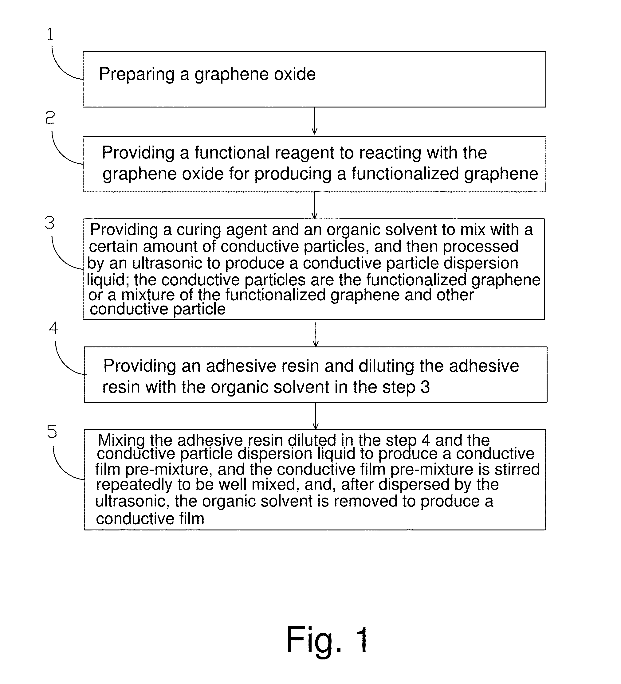
[0034]Please refer to FIG. 1. The present invention provides a method of manufacturing a conductive film, which comprises the steps as follows.

[0035]Step 1: preparing a graphene oxide; wherein the graphene oxide is prepared by Hummers method in the step 1.

[0036]Step 2: providing a functional reagent to reacting with the graphene oxide for producing a functionalized graphene.

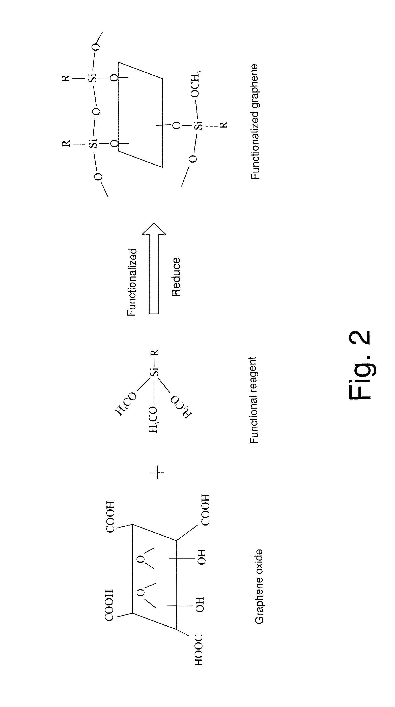
[0037]Please refer to FIG. 2. In the step 2, the functional reagent reacts with the functional groups on the surface of the graphene oxide to introduce the functionalized molecular onto the surface of the graphene oxide and reducing other oxygen functional groups on the surface of the graphene oxide to obtain the functionalized graphene. By introducing functionalized molecular having polar groups onto the surface of the functionalized graphene, distribution of the functionalized graphene in the adhesive resin can be improved.

[0038]A general structure of the functional reagent is:

wherein the structure of the radic...


PUM

PropertyMeasurementUnit
depthaaaaaaaaaa
conductiveaaaaaaaaaa
reduced pressureaaaaaaaaaa

Abstract

The present invention provides a method of manufacturing conductive film and the conductive film itself. The method of manufacturing conductive film comprises the following steps: step 1 for preparing a graphene oxide; step 2 for providing a functional reagent to reacting with the graphene oxide for producing a functionalized graphene; step 3 for providing a curing agent and an organic solvent to mix with a certain amount of conductive particles, and then processed by an ultrasonic to produce a conductive particle dispersion liquid; the conductive particles are the functionalized graphene or a mixture of the functionalized graphene and other conductive particle; step 4 for providing an adhesive resin and diluting the adhesive resin with the organic solvent in the step 3; step 5 for mixing the adhesive resin diluted in the step 4 and the conductive particle dispersion liquid to produce a conductive film pre-mixture, and the conductive film pre-mixture is stirred repeatedly to be well mixed, and, after dispersed by the ultrasonic, the organic solvent is removed to produce a conductive film.

Description

FIELD OF THE INVENTION[0001]The present invention relates to the technical field of liquid crystal display, and more particularly to a method of manufacturing a conductive film and the conductive film itself.BACKGROUND OF THE INVENTION[0002]Nowadays, a conductive film is mainly comprised of a polymer adhesive substrate and metal conductive filler for combining the conductive particles together by adhesive effect of the resin substrate to form a conductive path and realize a conductive connection between the adhered materials. The conductive particles used in the conductive film are usually metal powders of Au, Ag, Al, Cu, Ni, etc. Cu, Al and Ni are cheap and with good conductivity, however, they are easily to be oxidized in the air when the temperature is high such that the conductivity becomes poor and the stability and reliability is limited. The powder of Ag has good conductivity and chemical stability, and is hardly to be oxidized in the adhesive substrate, however, the density ...

Claims


Application Information

Patent Timeline
Patent Type & Authority Applications(United States)
IPC IPC(8): H01B1/24C09J7/10
CPCH01B1/24C09J9/02C09J11/04C08K9/04C08K2201/001C08K3/042C09J7/10C09J2301/314C09J2301/408
Inventor LEE, YUNGJUILI, JICHEN, YAHUI
Owner TCL CHINA STAR OPTOELECTRONICS TECH CO LTD
Why Eureka
Try Eureka