Processes for producing and treating thin-films composed of nanomaterials

a technology of nanomaterials and processes, applied in the field of nanomaterials, can solve the problems of high vacuum deposition, limited scalability, high cost, etc., and achieve the effect of reducing the resistivity of transparent conducting films

Active Publication Date: 2016-09-01
PURDUE RES FOUND INC
View PDF9 Cites 15 Cited by
  • Summary
  • Abstract
  • Description
  • Claims
  • Application Information

AI Technical Summary

Benefits of technology

The present invention is about methods for making and treating thin films made of nanomaterials. These methods include producing transparent conducting films, reducing the resistance of transparent conducting films, and combining nanomaterials with 2D materials.

Problems solved by technology

The patent text discusses the use of nanomaterials in thin-films and the challenges of integrating them onto other nanomaterials. The technical problem addressed is the lack of physical contact between the nanomaterials and graphene or other 2D materials, which degrades the out-of-plane electronic transport and chemical interactions between them. The patent aims to incorporate nanomaterials-based thin-films into various applications, including TCFs.

Method used


Image

  • Processes for producing and treating thin-films composed of nanomaterials
  • Processes for producing and treating thin-films composed of nanomaterials
  • Processes for producing and treating thin-films composed of nanomaterials

Examples


Embodiment Construction

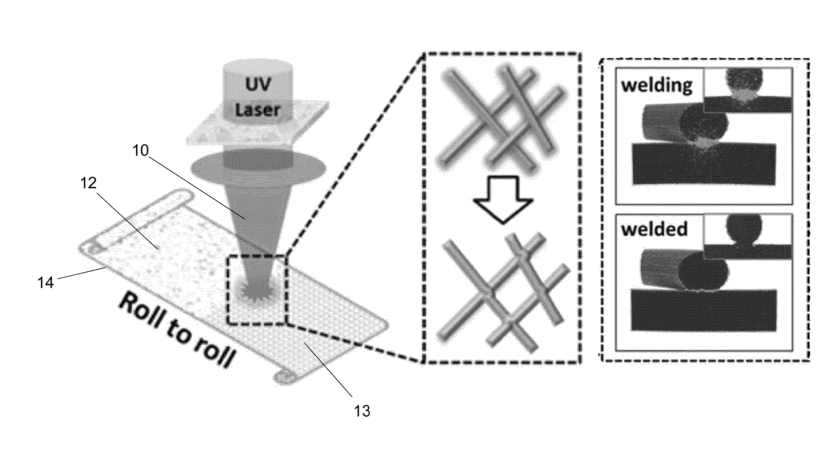
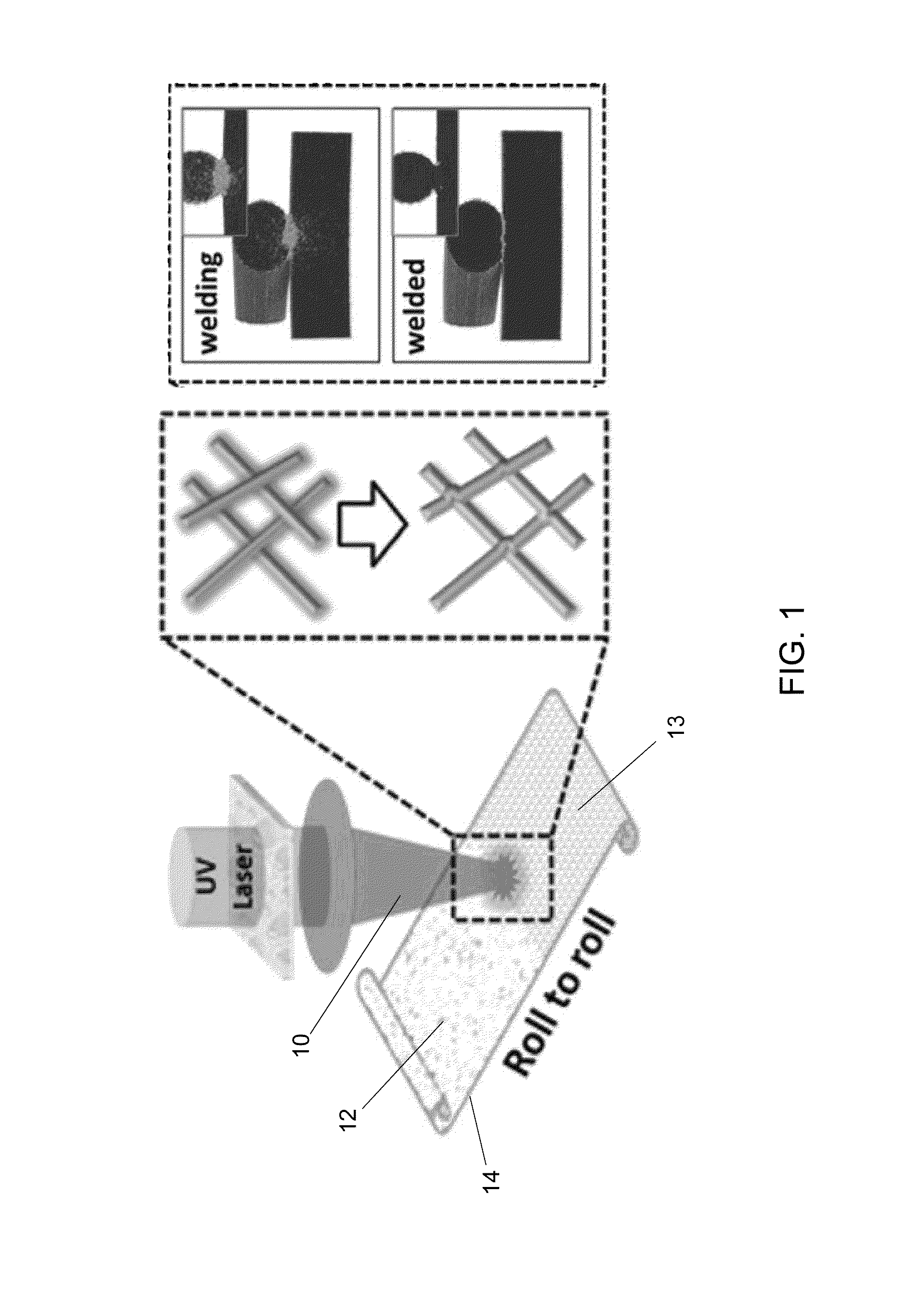
[0027]The present invention provides processes for producing and / or treating thin-films comprising nanomaterials, in particular by integrating 0D, 1D, 2D, and / or 3D nanomaterials together using laser or other high speed intensive optical source processing systems, particularly to join the nanomaterials by pulsed laser induced welding, or by laser shock induced integration.

[0028]In a first nonlimiting embodiment, a process is provided for joining or welding of conductive nanomaterials, particularly 1D metallic materials including nanowires, for example, to produce transparent conducting films (TCFs) formed entirely of the conductive nanomaterials.

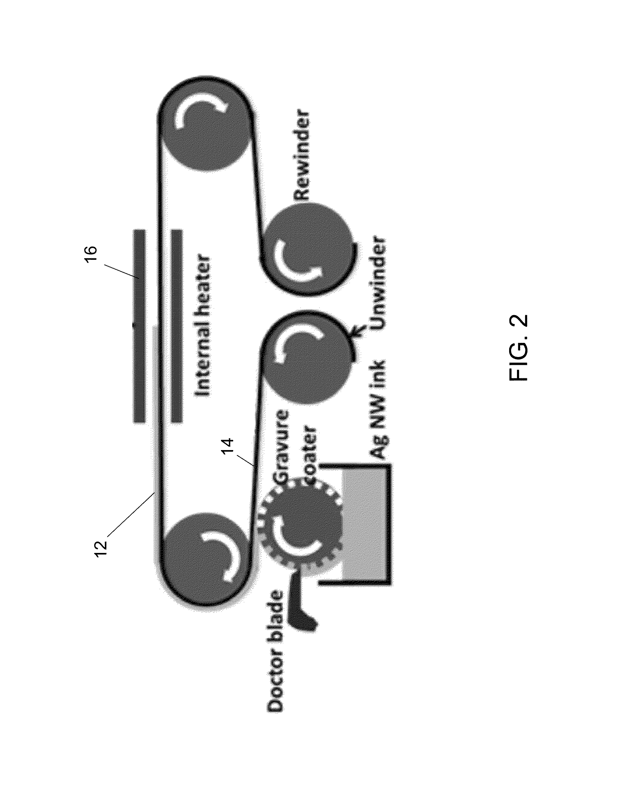
[0029]Such a process includes laser heating one or more layers of conductive nanomaterials, for example nanowires, that have been printed on a substrate as a thin-film. Preferably, such a technique involves direct laser welding of a printed conductive nanowire network that has been applied by a roll-to-roll printing process to a flexible sub...


PUM

PropertyMeasurementUnit
Pressureaaaaaaaaaa
Electrical conductoraaaaaaaaaa
Transparencyaaaaaaaaaa

Abstract

Processes for producing and treating thin-films comprising nanomaterials are provided. A process of producing a transparent conducting film includes printing nanomaterials on a substrate, and directing a laser beam onto the nanomaterials to weld junctions between the nanomaterials. A process for tightly integrating nanomaterials with 2D material includes locating the 2D material over the nanomaterials, and directing a laser beam towards the 2D material to produce laser shock pressure sufficient to wrap the 2D material on the nanomaterials. A process of reducing the resistivity of a transparent conducting film includes directing a first laser beam towards a transparent conducting film having nanomaterials thereon such that the nanomaterials experience laser shock pressure sufficient to compress the nanomaterials, and then directing a second laser beam towards the transparent conducting film such that junctions between the nanomaterials are fused.

Description


Claims


Application Information

Patent Timeline
Owner PURDUE RES FOUND INC
Why Eureka
Try Eureka