Display panel with touch detection function

a display panel and touch detection technology, applied in the field of display panel with touch detection function, can solve the problems of increased product cost, increased manufacturing process, increased product cost, etc., and achieve the effects of increasing the number of wiring layers, increasing the product cost, and complicated manufacturing process

Inactive Publication Date: 2016-09-01
PANASONIC LIQUID CRYSTAL DISPLAY CO LTD +1
View PDF14 Cites 32 Cited by
  • Summary
  • Abstract
  • Description
  • Claims
  • Application Information

AI Technical Summary

Benefits of technology

[0005]However, in the technology disclosed in the above-mentioned publication, the following two problems mainly arise. The first problem resides in that the manufacturing process is complicated, and hence the product cost is increased. FIG. 32 is a plan view of a display panel disclosed in the above-mentioned publication. As illustrated in FIG. 32, when a sensor electrode line 706 is formed in a different layer from that of a source line 704, the number of wiring layers is increased. With this, the manufacturing process is complicated, and the product cost is increased. The second problem resides in reduction in detection accuracy of a touch position. As illustrated in FIG. 32, when the sensor electrode line 706 is formed in proximity to the source line 704, the sensor electrode line 706 is susceptible to an electric field from the source line 704. In this case, the detection accuracy of the touch position is remarkably reduced due to the influence of the above-mentioned electric field.

Problems solved by technology

However, in the technology disclosed in the above-mentioned publication, the following two problems mainly arise.
The first problem resides in that the manufacturing process is complicated, and hence the product cost is increased. FIG. 32 is a plan view of a display panel disclosed in the above-mentioned publication.
With this, the manufacturing process is complicated, and the product cost is increased.
The second problem resides in reduction in detection accuracy of a touch position.

Method used


Image

  • Display panel with touch detection function
  • Display panel with touch detection function
  • Display panel with touch detection function

Examples


first embodiment

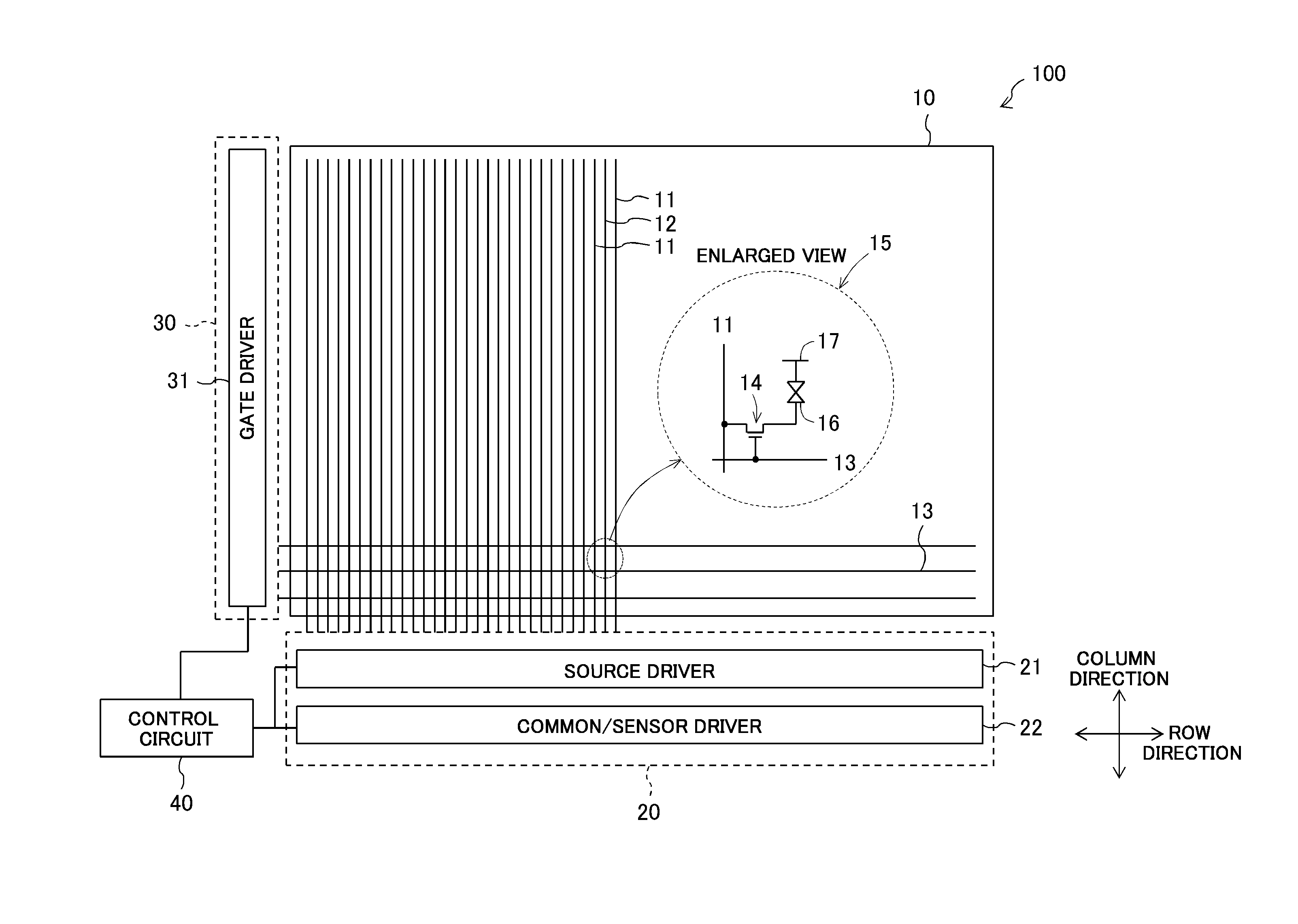
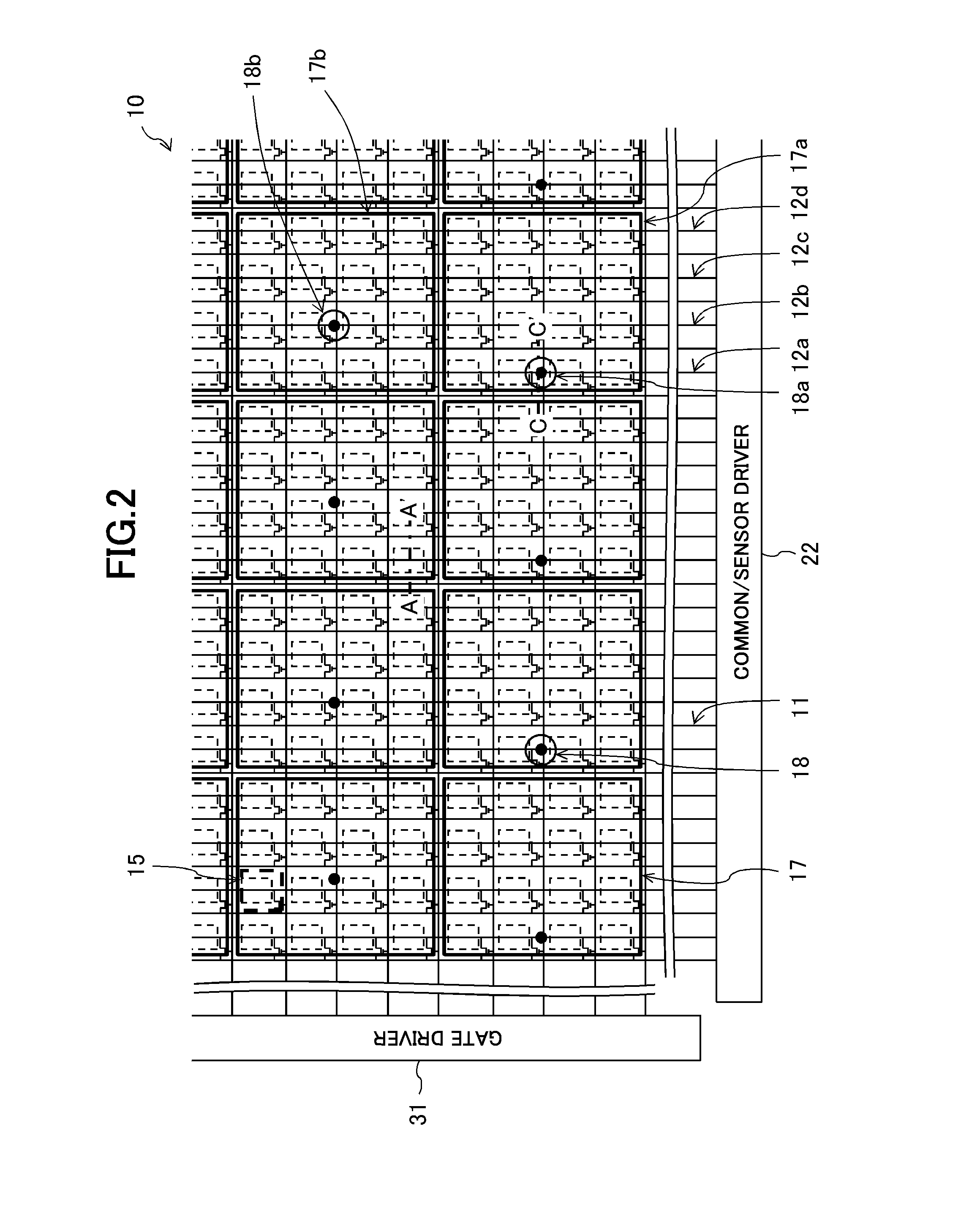
[0057]FIG. 2 is a plan view illustrating details of a display panel 10 of the first embodiment. In FIG. 2, for the sake of easy understanding of the description, the source driver 21 is omitted. In the configuration illustrated in FIG. 2, the plurality of common electrodes 17 are arranged at a ratio of one to a total of sixteen pixels 15 including four pixels 15 in the column direction and four pixels 15 in the row direction. The plurality of common electrodes 17 each have the substantially same shape, and are arrayed regularly. The sensor electrode lines 12 are arranged in the TFT substrate between adjacent two of the data signal lines 11 in plan view. In plan view, each of the common electrodes 17 overlaps with the plurality of sensor electrode lines 12, and is electrically connected to one of the plurality of sensor electrode lines 12 via a through hole (contact hole) 18. In the configuration illustrated in FIG. 2, a common electrode 17a overlaps with four sensor electrode lines ...

second embodiment

[0066]FIG. 5 is a plan view illustrating details of a display panel 10 of the second embodiment. In FIG. 5, for the sake of easy understanding of the description, the source driver 21 is omitted. In the TFT substrate, the sensor electrode line 12 is arranged between adjacent two of the data signal lines 11 in plan view. Further, the sensor electrode line 12 is arranged in each of a red pixel (R pixel) for displaying red and a blue pixel (B pixel) for displaying blue, but is not arranged in a green pixel (G pixel) for displaying green. Further, in plan view, each of the common electrodes 17 overlaps with the plurality of sensor electrode lines 12, and is electrically connected to one of the plurality of sensor electrode lines 12 via the through hole (contact hole) 18. In the configuration illustrated in FIG. 5, the common electrode 17a overlaps with three sensor electrode lines 12a, 12c, and 12d, and is electrically connected to one sensor electrode line 12a among those sensor electr...

third embodiment

[0073]FIG. 10 is a sectional view taken along the line C-C′ of FIG. 2 in a display panel 10 of the third embodiment. Note that, in FIG. 2, the slits 17s are omitted.

[0074]In the TFT substrate 200, the plurality of gate signal lines 13 (not shown) are formed on the glass substrate 201, the first insulating film 202 is formed so as to cover the plurality of gate signal lines 13, and the plurality of data signal lines 11, the plurality of pixel electrodes 16, and the plurality of sensor electrode lines 12 are formed in the same layer on the first insulating film 202. The second insulating film 203 is formed so as to cover the plurality of data signal lines 11, the plurality of pixel electrodes 16, and the plurality of sensor electrode lines 12, and the through hole 18 is formed through a part of the second insulating film 203. The plurality of common electrodes 17 are formed on the second insulating film 203 and inside the through hole 18. The sensor electrode line 12 is electrically c...


PUM


Abstract

Provided is a display panel including: a plurality of pixel electrodes divided into a plurality of groups; and a plurality of common electrodes arranged at a ratio of one to a plurality of pixel electrodes included in one of the plurality of groups. A plurality of sensor electrode lines are arranged in the same layer as a plurality of data signal lines. The plurality of sensor electrode lines and each of the plurality of common electrodes overlap each other in plan view. The each of the plurality of common electrodes is electrically connected to at least one of the plurality of sensor electrode lines. At least one insulating film is formed between each of a region between the data signal lines and the sensor electrode lines, a region between the sensor electrode lines and the common electrodes, and a region between the common electrodes and the pixel electrodes.

Description

BACKGROUND[0001]1. Field of the Invention[0002]The present application relates to a display panel with touch detection function.[0003]2. Description of the Related Art[0004]Hitherto, various display devices with touch panels have been proposed. In recent years, in order to reduce the thickness of the entire display device, there has been proposed a so-called in-cell display device with touch detection function, which incorporates a function of a touch panel inside a display panel. The above-mentioned display device is disclosed in, for example, U.S. Pat. No. 8,766,950. Further, in the above-mentioned publication, there is disclosed an in-plane switching (IPS) display panel that is excellent in wide viewing angle characteristics.SUMMARY[0005]However, in the technology disclosed in the above-mentioned publication, the following two problems mainly arise. The first problem resides in that the manufacturing process is complicated, and hence the product cost is increased. FIG. 32 is a pl...

Claims


Application Information

Patent Timeline
Patent Type & Authority Applications(United States)
IPC IPC(8): G06F3/041G06F3/044
CPCG06F3/044G06F3/0416G06F3/0412G09G3/3648G06F3/04164G06F3/0443
Inventor AOYAMA, TOSHIYUKIFUKAMI, TETSUOKAJITA, DAISUKETAKAGI, KAZUSHIGE
Owner PANASONIC LIQUID CRYSTAL DISPLAY CO LTD
Why Eureka
Try Eureka