Method for producing substrates for superconducting layers
a superconducting layer and substrate technology, applied in the direction of superconducting device, superconducting details, cable/conductors, etc., can solve the problem of not being able to adapt to continuous processing of long lengths of such tape, and achieve the effect of large degree of control
- Summary
- Abstract
- Description
- Claims
- Application Information
AI Technical Summary
Benefits of technology
Problems solved by technology
Method used
Image

Examples
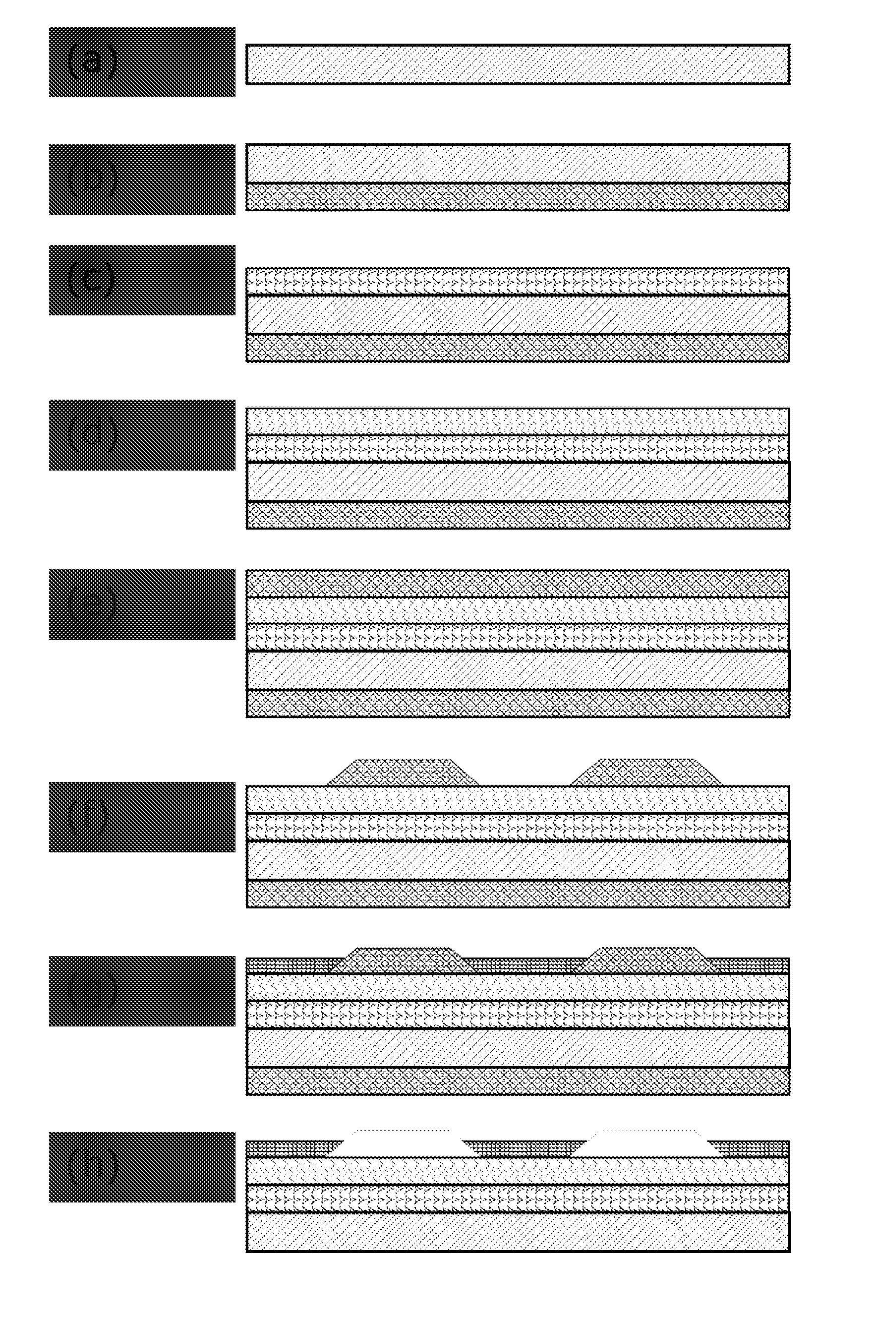
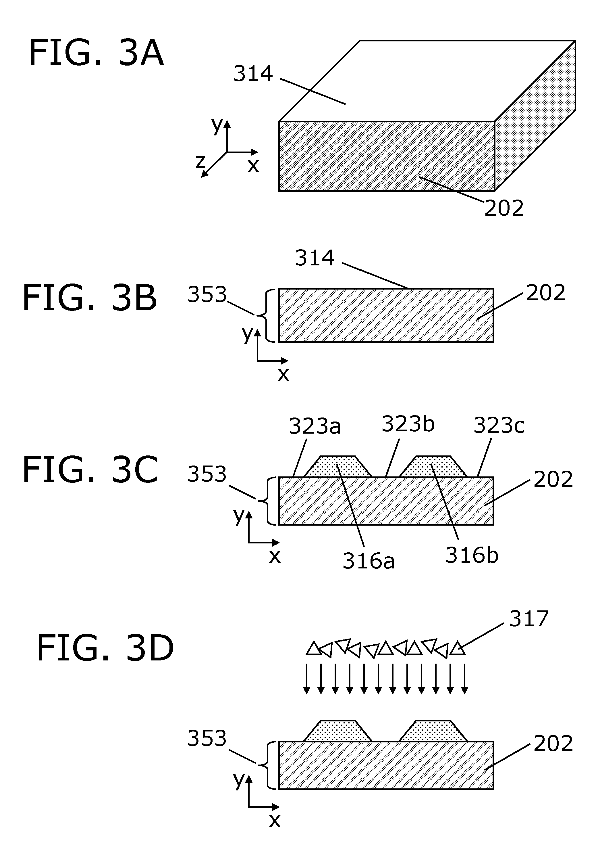
example a
[0180]In an exemplary embodiment according to the invention, there may be provided a substrate suitable for supporting an elongated superconducting element according to the following protocol, which protocol describes copper plating strips with a shadow-profile on Hastelloy C276 metal tapes.[0181]1) The solid element is provided in form of a metal tape (Hastelloy C276) which is cleaned applying an alkaline soak, or alternatively, 5 min cleaning in acetone with ultrasound and then 5 min in ethanol with ultrasound.[0182]2) Placing one or more strips of masking material is carried out with Kapton® masking tape which is applied in parallel strips on the up side of the metal tape and smoothened so that there are no air bubbles between the Kapton® tape and the metal tape. The edges of the Kapton® tape are cut so that the down side of the tape (glue side) is wider than the up side and preferably so that one or both edges make an angle of about 45° with the tape plane (e.g., such as depicte...
example b
[0200]A layer of masking material is provided by a protective layer, such as a standard imprint resist or photoresist for UV lithography, a Kapton® film or scotch tape.
[0201]The layer of masking material of e.g. photoresist (produced e.g. using die slot coating or dip coating) or Kapton® film, or imprint resist or scotch tape is applied to the sample surface (i.e., to the surface of the solid element). Forming elongated strips of masking material is carried out by cutting or roll-cutting lines into the layer of masking material and subsequently removing, e.g., every second of the thin strips of layer of masking material so that the surface of the solid element is (partially) covered by parallel but separated, elongated strips of masking material, e.g. strips of Kapton® film.
example c
[0202]The starting material, such as the solid element (e.g. a Hastelloy tape), is coated with elgonated strips of masking material, such as with Kapton® film (or wax or lacquer) in stripes parallel to the length of the metal tape. The stripes should be e.g. 1 mm wide and positioned with a spacing of, e.g., 1 mm. Notice that the Kapton® film may be firmly attached to the sample, e.g. using a brush or rubber rolls. Masking material, such as protective lacquer or wax, may be coated in parallel lines using a slot die coater or an alternative standard coating process. This lacquer or wax can subsequently be removed using e.g. acetone or hot water.
PUM
| Property | Measurement | Unit |
|---|---|---|
| length | aaaaa | aaaaa |
| length | aaaaa | aaaaa |
| length | aaaaa | aaaaa |
Abstract
Description
Claims
Application Information
PatSnap Eureka turns technology decisions into work you can execute. Powered by our Innovation Knowledge Graph, it runs expert workflows across engineering, life sciences, materials and intellectual property. Get your review-ready output in minutes.


