Lead frame for mounting semiconductor element and method for manufacturing the same

Active Publication Date: 2016-09-22
OHKUCHI MATERIALS CO LTD
View PDF10 Cites 4 Cited by
  • Summary
  • Abstract
  • Description
  • Claims
  • Application Information

AI Technical Summary

Benefits of technology

The invention provides a semiconductor-mounting part or terminal part with a protrusion that runs horizontally and vertically, making it tolerant to stress in all directions and improving the contact area between metal substrate and resin. This prevents the resin from peeling off from the metal substrate due to thermal or vamental stresses during the cutting process.

Problems solved by technology

However, the trouble which is acknowledged as problem in the present field is that resin inevitably peels off from a lead frame because of influences of: expansion or contraction of resin due to thermal history at high temperatures; and vibration, the expansion or contraction and vibration occurring due to friction between a lead frame sheet and a blade when the lead frame sheet is cut off into strips.

Method used


Image

  • Lead frame for mounting semiconductor element and method for manufacturing the same
  • Lead frame for mounting semiconductor element and method for manufacturing the same
  • Lead frame for mounting semiconductor element and method for manufacturing the same

Examples


embodiment 1

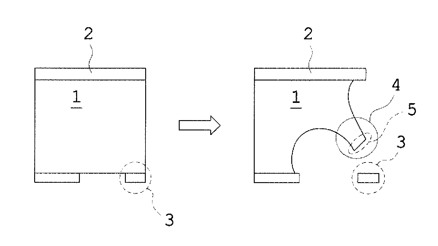
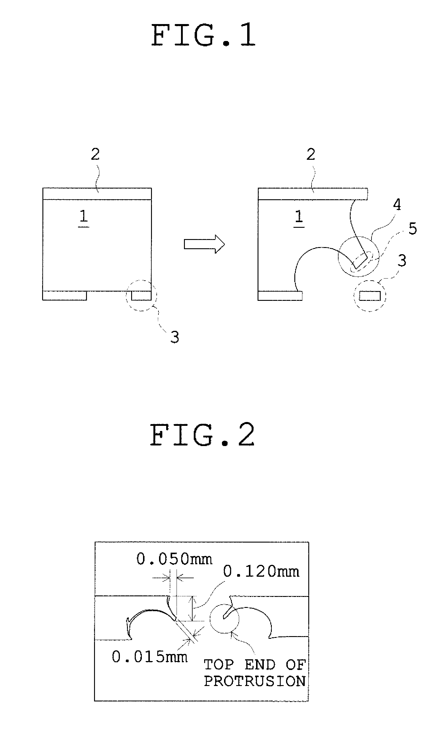
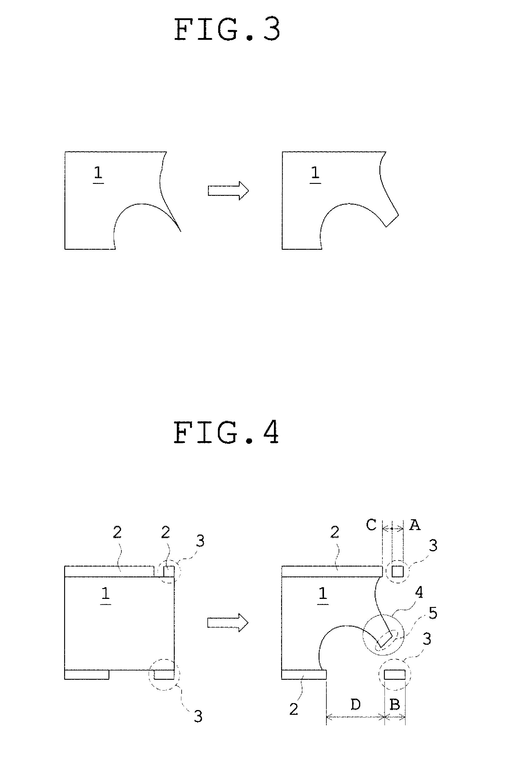
[0027]A band-shaped cupper material (KLF-194: made by Kobe Steel, Ltd.) having a thickness of 0.2 mm and a width of 180 mm was used as a metal substrate 1 for lead frame, and photo sensitive resist layers (negative-type photo sensitive resist AQ-2058: made by Asahi Kasei E-materials Corporation.) each having a thickness of 20 μm were formed on the both surfaces of this metal substrate respectively. And then, in order to form a protrusion 4, the both surfaces of the metal substrate 1 that were given the photo sensitive resist layers respectively were exposed to be developed through glass masks (HY2-50P: made by KONIKA MINOLTA ADVANCED LAYERS, INC.), one of the glass masks having been given a design for lead frame which included a pattern for forming an etching resist pattern layer having a width A of 40 μm on the packaging-surface side and the other of the glass masks having been given a design for lead frame which included a pattern for forming an etching resist pattern layer having...

embodiment 2

[0028]A band-shaped cupper material (KLF-194: made by Kobe Steel, Ltd.) having a thickness of 0.2 mm and a width of 180 mm was used as a metal substrate 1 for lead frame, and photo sensitive resist layers (negative-type photo sensitive resist AQ-2058: made by Asahi Kasei E-materials Corporation.) each having a thickness of 20 μm were formed on the both surfaces of this metal substrate 1 respectively. And then, in order to form a protrusion 4, the both surfaces of the metal substrate 1 that were given the photo sensitive resist layers respectively were exposed to be developed through glass masks (HY2-50P: made by KONIKA MINOLTA ADVANCED LAYERS, INC.), one of the glass masks having been given a design for lead frame which included a pattern for forming an etching resist pattern layer 3 having a width B of 90 μm only on the surface side which was exposed to the outside after sealing with resin, so that an etching resist pattern layer for lead frame having an etching resist pattern for ...

embodiment 3

[0029]A band-shaped cupper material (KLF-194: made by Kobe Steel, Ltd.) having a thickness of 0.2 mm and a width of 180 mm was used as a metal substrate 1 for lead frame, and photo sensitive resist layers (negative-type photo sensitive resist AQ-2058: made by Asahi Kasei E-materials Corporation.) each having a thickness of 20 μm were formed on the both surfaces of this metal substrate 1 respectively. And then, in order to form a protrusion 4, the both surfaces of the metal substrate 1 that were given the photo sensitive resist layers respectively were exposed to be developed through glass masks (HY2-50P: made by KONIKA MINOLTA ADVANCED LAYERS, INC.), one of the glass masks having been given a design for lead frame which included a pattern for forming an etching resist pattern layer having a width A of 55 μm on the packaging-surface side and the other of the glass masks having been given a design for lead frame which included a pattern for forming an etching resist pattern layer havi...


PUM


Abstract

A lead frame for mounting semiconductor element includes a protrusion that is horizontally projects from edges of the upper and lower surfaces of a semiconductor-mounting part or a terminal part of the lead frame and that is provided on a lateral side of at least one of the semiconductor-mounting part or the terminal part of the lead frame, wherein the top end of the protrusion is substantially flat or the profile of the cross section of the top end is arc-shaped, and the top end of the protrusion is thick.

Description

CROSS-REFERENCE TO RELATED APPLICATION[0001]This is a U.S. national phase application under 35 U.S.C §371 of International Patent Application No. PCT / JP2014 / 057315, filed on Mar. 18, 2014, and claims benefit of priority of Japanese Patent Application No. JP 2013-055771, filed on Mar. 18, 2013. The international Application was published on Sep. 25, 2014, as International Publication No. WO 2014 / 148484 under PCT Article 21(2). The entire contents of these applications are hereby incorporated herein by reference.FIELD OF THE INVENTION[0002]This invention relates to a lead frame for mounting semiconductor element, particularly, to the shapes of a semiconductor mounting part and a terminal part of the lead frame.BACKGROUND OF THE INVENTION[0003]For lead frames on which semiconductor elements are mounted, it is one of the important points for improving the reliability of products to improve adhesiveness of sealing resin to the terminal parts that are connected to semiconductor elements a...

Claims


Application Information

Patent Timeline
IPC IPC(8): H01L23/495H01L21/48
CPCH01L23/49548H01L21/4828H01L23/4952H01L23/49503H01L23/49541H01L23/49582H01L2924/0002H01L2924/00
Inventor YOSHIMOTO, RYOUICHIYAMASHITA, RYOHEI
Owner OHKUCHI MATERIALS CO LTD
Why Eureka
Try Eureka