

Light emitting component
a technology of light-emitting components and components, applied in the direction of basic electric elements, electrical equipment, semiconductor devices, etc., can solve the problems of limited light output and accordingly, and achieve the effects of enhancing the quantity of light output, reducing total reflection, and reducing light intensity
- Summary
- Abstract
- Description
- Claims
- Application Information
AI Technical Summary
Benefits of technology
Problems solved by technology
Method used
Image

Examples
first embodiment
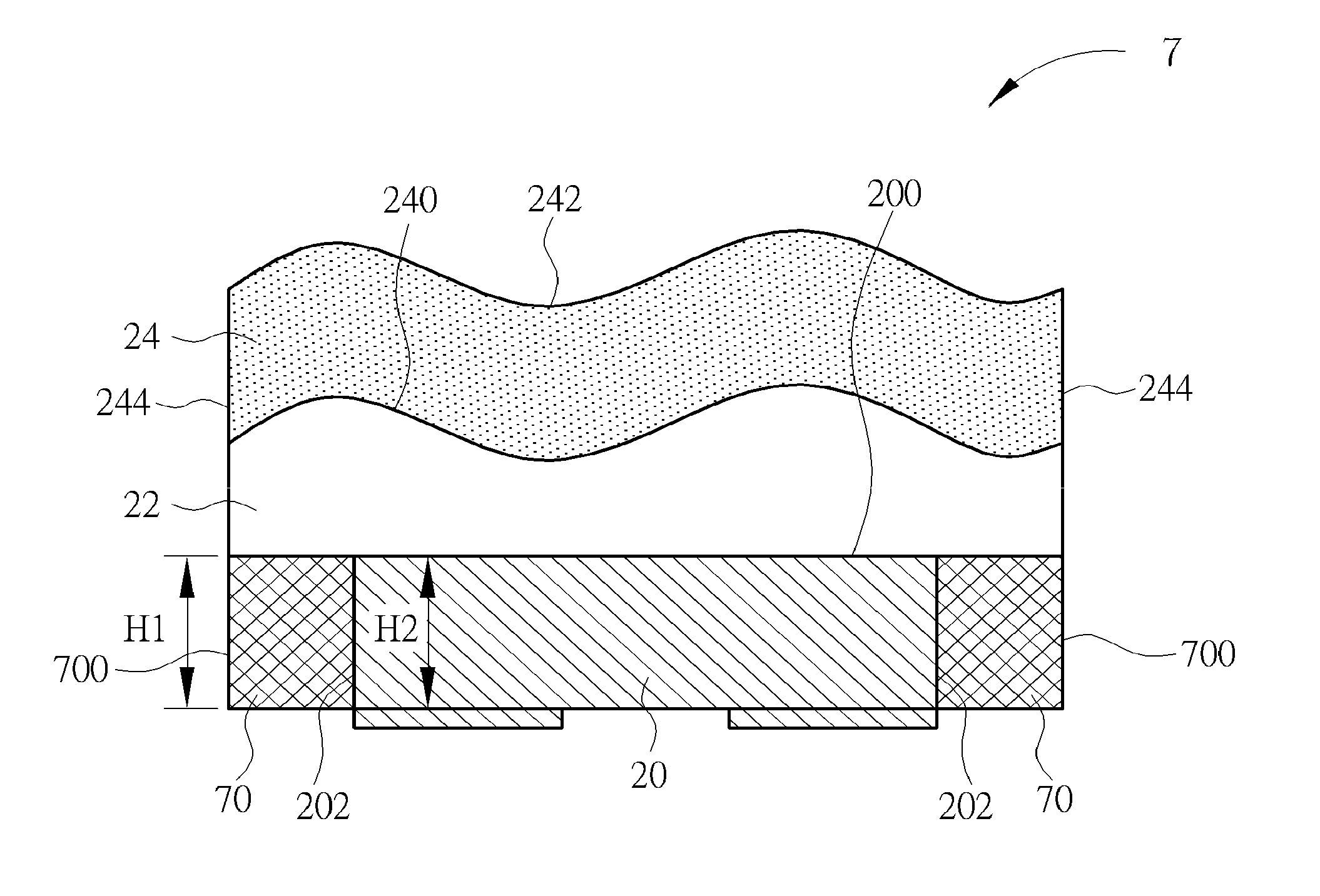
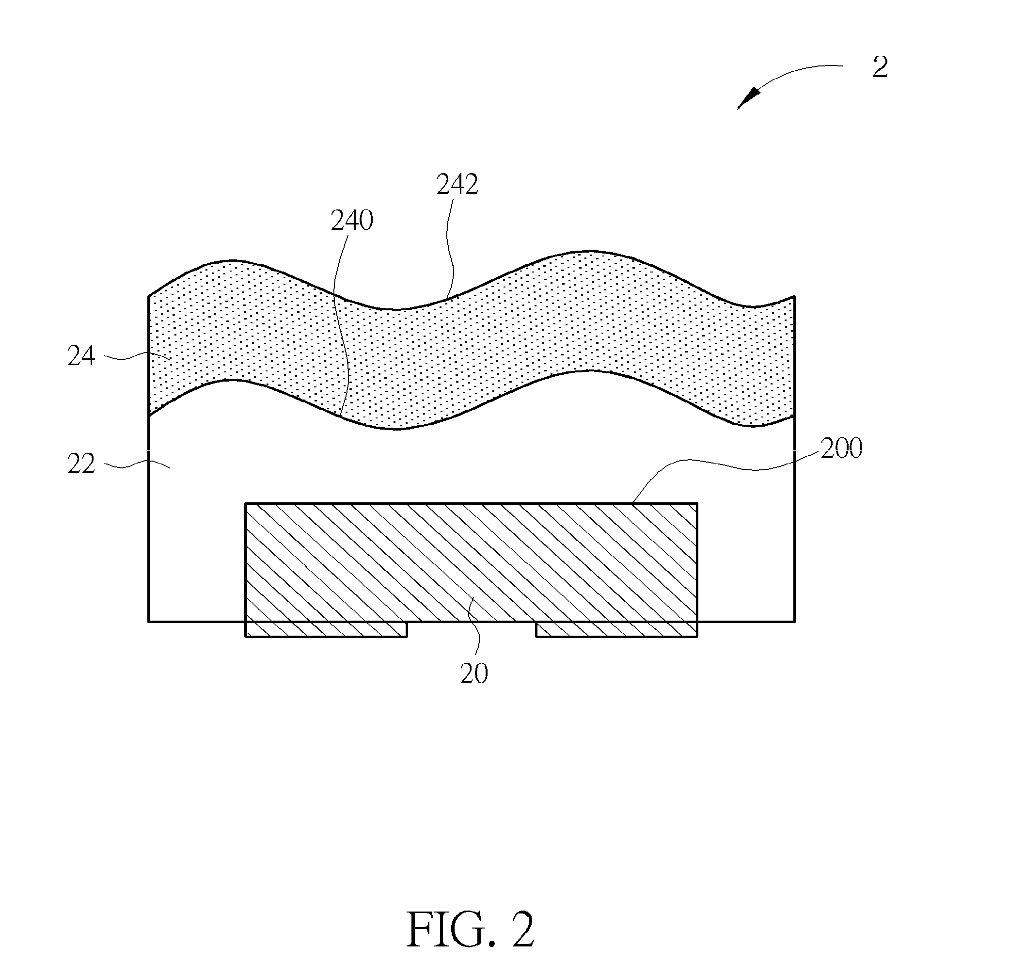
[0023]Referring to FIG. 2, FIG. 2 is a schematic view illustrating a light emitting component 2 according to the invention. As shown in FIG. 2, the light emitting component 2 comprises a light emitting unit 20, a molding compound 22 and a wavelength converting layer 24. The light emitting unit 20 has a forward light emitting surface 200. The molding compound 22 covers the light emitting unit 20. The wavelength converting layer 24 is disposed above the molding compound 22. The wavelength converting layer 24 has a first surface 240 and a second surface 242 opposite to the first surface 240, wherein the first surface 240 is located between the forward light emitting surface 200 and the second surface 242.
[0024]In this embodiment, the light emitting unit 20 may be, but not limited to, a light emitting diode. A material of the molding compound 22 may be silicone, epoxy or other molding compounds. The wavelength converting layer 24 may be made of a mixture of a transparent glue and phosph...
second embodiment
[0027]Referring to FIG. 3 along with FIG. 2, FIG. 3 is a schematic view illustrating a light emitting component 3 according to the invention. The main difference between the light emitting component 3 and the aforesaid light emitting component 2 is that the second surface 242 of the wavelength converting layer 24 of the light emitting component 3 is planar. It should be noted that the same elements in FIG. 3 and FIG. 2 are represented by the same numerals, so the repeated explanation will not be depicted herein again.
third embodiment
[0028]Referring to FIG. 4 along with FIG. 2, FIG. 4 is a schematic view illustrating a light emitting component 4 according to the invention. The main difference between the light emitting component 4 and the aforesaid light emitting component 2 is that the first surface 240 of the wavelength converting layer 24 of the light emitting unit 4 is planar. It should be noted that the same elements in FIG. 4 and FIG. 2 are represented by the same numerals, so the repeated explanation will not be depicted herein again.
[0029]As the light emitting components 2, 3 and 4 shown in FIGS. 2 to 4, the invention may make at least one of the first surface 240 and the second surface 242 of the wavelength converting layer 24 to be non-planar according to practical applications. When the first surface 240 of the wavelength converting layer 24, which contacts the molding compound 22, is non-planar, the contact area between the wavelength converting layer 24 and the molding compound 22 increases (e.g. th...
PUM
 Abstract
Description
Claims
Application Information