Digital imaging and pulse detection pixel

a digital imaging and pulse detection technology, applied in the field of image sensing and pulse detection circuitry, can solve the problems of increasing the weight of the pixel array and the lager pixel siz

Active Publication Date: 2016-10-06
HAMILTON SUNDSTRAND CORP
View PDF3 Cites 68 Cited by
  • Summary
  • Abstract
  • Description
  • Claims
  • Application Information

AI Technical Summary

Problems solved by technology

The dual chip configuration of existing pixels results in...

Method used


Image

  • Digital imaging and pulse detection pixel
  • Digital imaging and pulse detection pixel
  • Digital imaging and pulse detection pixel

Examples


Embodiment Construction

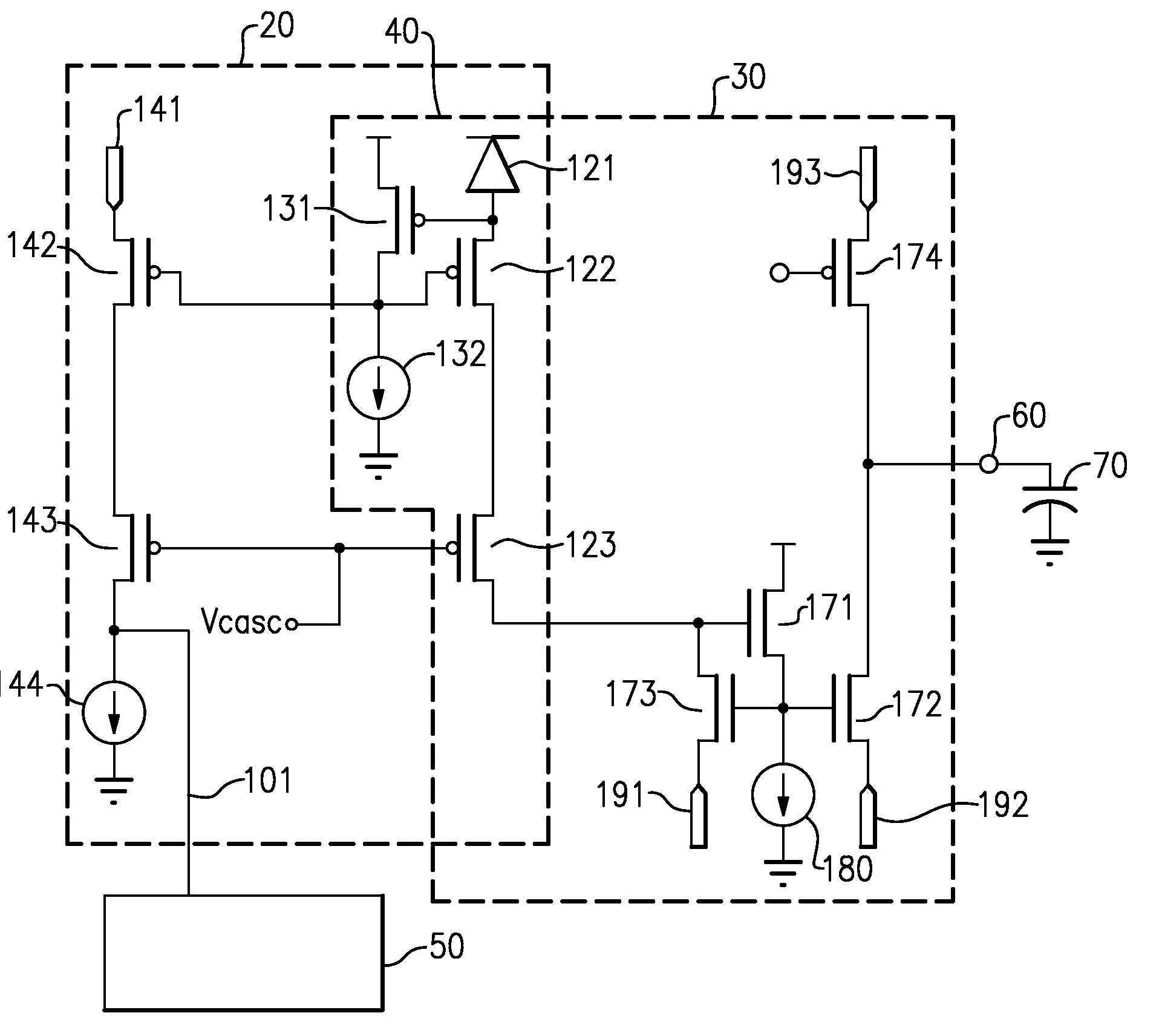
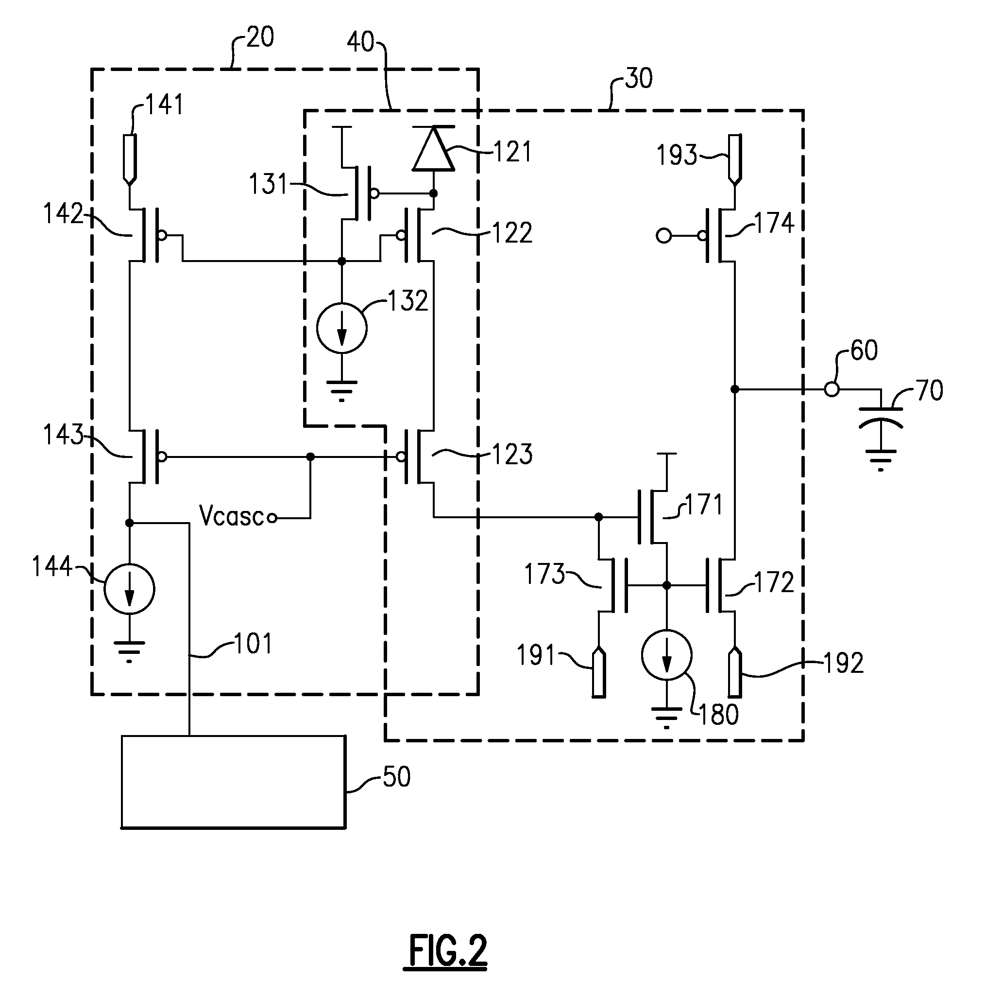
[0010]Imaging systems, including imaging systems with laser pulse detection features, utilize an array of pixels to capture and analyze an image. Typically within each array, every pixel is approximately identical. In some exemplary pixel arrays, each pixel includes a pulse detection system and an imaging system.

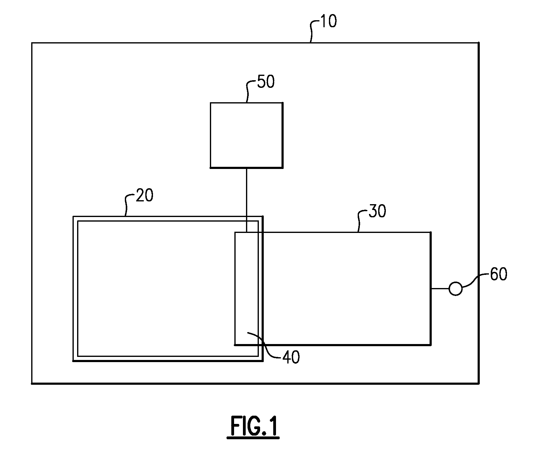
[0011]FIG. 1 schematically illustrates a pixel 10 for utilization in an imaging system with laser pulse detection. The pixel 10 includes a pulse detection circuit 20 and an imaging circuit 30. Also included within the pixel 10 is a pulse processing circuit 50 connected to one or both of the imaging circuit 30 and the pulse detection circuit 20. In the example pixel 10 of FIG. 1, the pulse detection circuit 20 and the imaging circuit 30 utilize the same circuit architecture and are mounted on a single integrated circuit chip. In some examples, the single integrated circuit chip can be a readout integrated circuit (ROIC) chip. In alternative examples, the single integrated cir...


PUM


Abstract

An imaging and pulse detection array includes: a plurality of pixels connected to a controller, the controller being configured to generate an image based on an image signal originating from each pixel in the plurality of pixels and configured to detect a pulse on at least one of the pixels in the plurality of pixels, and each of the pixels in the plurality of pixels including an imaging circuit and a pulse detection circuit, the imaging circuit and the pulse detection circuit including a shared circuit architecture, and wherein the imaging circuit and the pulse detection circuit include a shared portion.

Description

TECHNICAL FIELD[0001]The present disclosure relates generally to image sensing and pulse detection circuitry, and more particularly to an implementation of an imaging pixel including imaging sensing and pulse detection on a single chip.BACKGROUND[0002]Infrared detector systems, LIDAR (laser illuminated detection and ranging) systems, and imaging systems in industrial processes utilize imaging pixel arrays and pulse detection pixel arrays to detect the presence of a laser pulse within an image. The properties of the laser pulse can then be analyzed by a controller to determine pertinent information such as a distance of the laser pulse, the time period of the laser pulse, or any other information needed by the controller.[0003]Existing imaging and pulse detecting systems utilize distinct imaging circuits and pulse detection circuits, with each of the circuits have different architectures. Due to the distinct architectures, the imaging portion and the pulse detection portion do not in...

Claims


Application Information

Patent Timeline
IPC IPC(8): H01L27/146G01S7/4863G01S17/86
CPCH01L27/14643H01L27/14609G01S7/4804G01S7/4863G01S17/86G01J1/00G01L27/00G01T1/20
Inventor LIN, MINLONGLUND, JOSHUA
Owner HAMILTON SUNDSTRAND CORP
Why Eureka
Try Eureka