
Pixel structure

a pixel structure and pixel technology, applied in the field of display, can solve problems such as adversely affecting image resolution

Active Publication Date: 2016-10-27
EVERDISPLAY OPTRONICS (SHANGHAI) CO LTD
View PDF34 Cites 6 Cited by
  • Summary
  • Abstract
  • Description
  • Claims
  • Application Information

AI Technical Summary

Benefits of technology

The present invention provides a pixel structure that solves the problem of low resolution in conventional techniques by reducing the number of signal lines occupying the sub pixel space. The scan signal line of the current row of pixel units is led by a corresponding connection signal line of the third metal wire layer to the second scan signal line of the next row of pixel units and severs as the second scan signal of the next row of pixel units. This eliminates one scan signal line in the pixel structure and increases the pixel resolution (up to 6,000 PPI) without compromising the demand burden on the integrated circuit. Additionally, a second capacitor is formed to increase the effective capacitance of the pixel structure and compensate for the deficiency of reduced capacitance resulting from a high resolution.

Problems solved by technology

Since the four signal lines occupy most of the sub pixel space, the pixels per inch (PPI) is not high and, thus, adversely affects the image resolution.

Method used


Image

  • Pixel structure
  • Pixel structure
  • Pixel structure

Examples


Embodiment Construction

[0036]The present invention will be described further in connection with the accompanying drawings and specific embodiments.

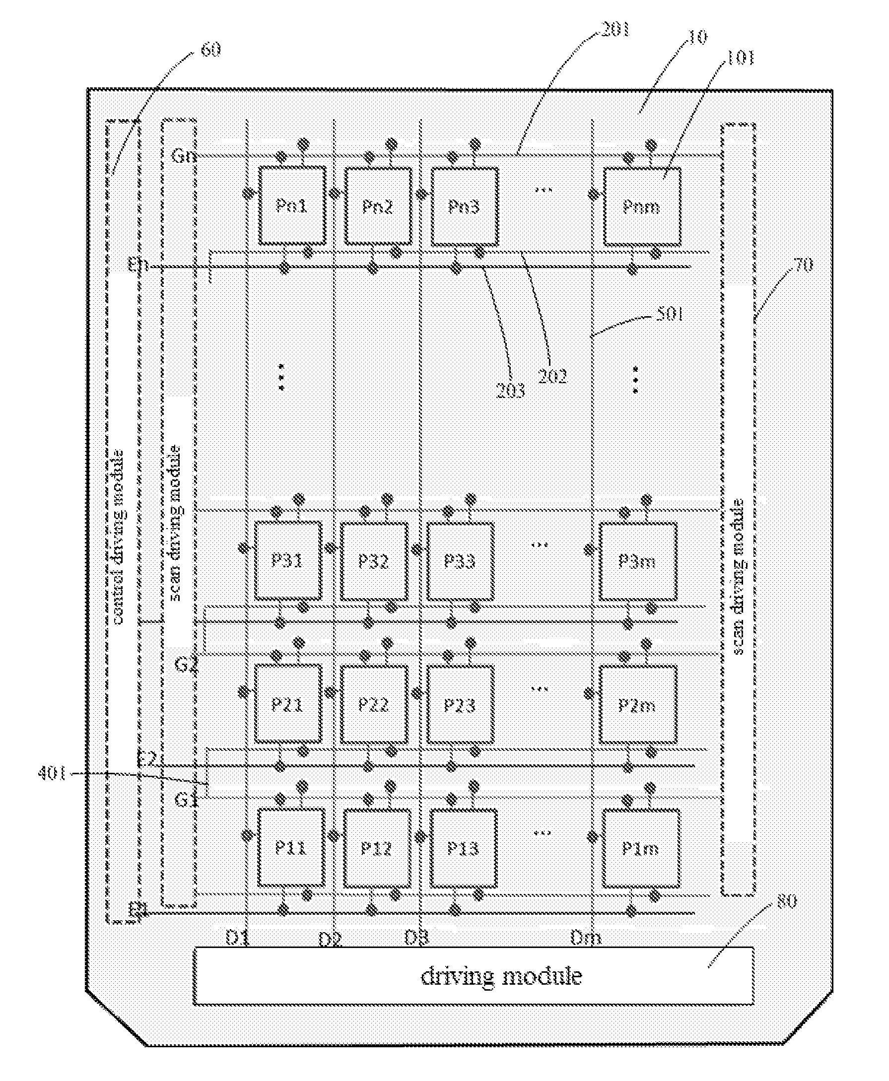
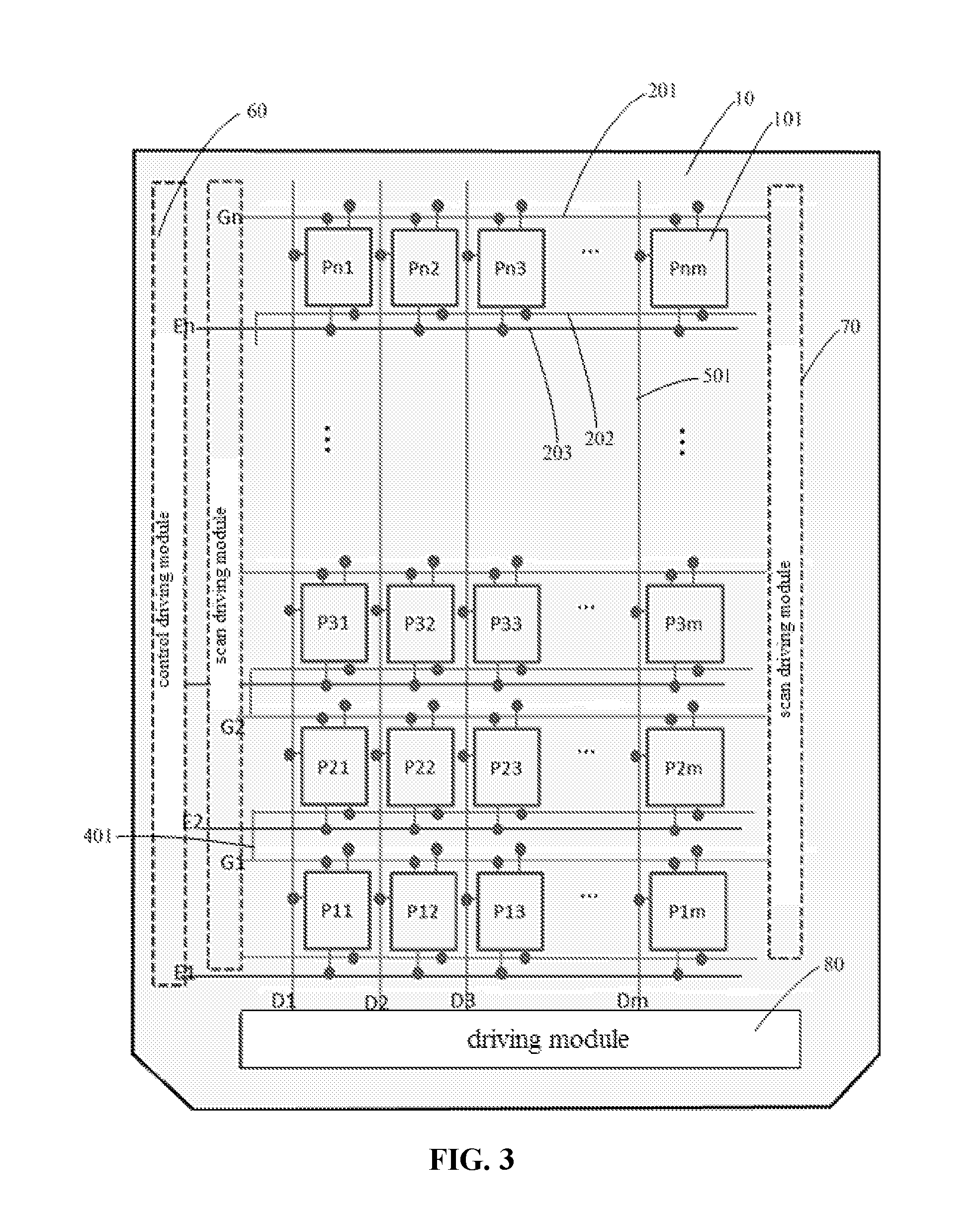
[0037]FIG. 3 is a gate driver on array (GOA) circuit of a pixel structure according to the present invention. The pixel structure includes a pixel unit layer 10 including a pixel unit array having a plurality of rows of pixel units 101 and a plurality of columns of pixel units 101. Each row of pixel units 101 and each row of pixel units 101 extend in a horizontal direction and a vertical direction, respectively.

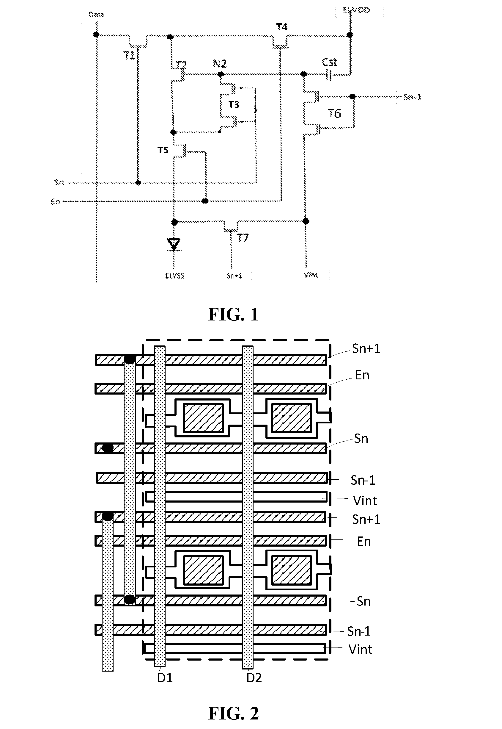
[0038]With reference to FIG. 5, the pixel structure further includes a first metal wire layer 20, a second metal wire layer 30, and a third metal wire layer 40.

[0039]With reference to FIG. 4, the first metal wire layer 20 includes a plurality of control signal lines 203, a plurality of first scan signal lines 201, a plurality of second scan signal lines 202, and a plurality of first metal patterned sections 204. Each of the control signal lines 203, the ...


PUM


Abstract

A pixel structure includes a pixel unit layer and a first metal wire layer. Each of control signal line and first and second scan signal lines in the first metal wire layer is connected to each pixel unit in a corresponding row. An insulating layer is disposed between each first metal patterned section in the first metal wire layer and a corresponding row of pixel units. A second metal wire layer includes initial signal lines and second metal patterned sections. Each initial signal line is connected to each pixel unit in a corresponding row. Each second metal patterned section overlaps with one of the first metal patterned sections to form a capacitor. Each connection signal line in a third metal wire layer connects the first scan signal line of a current row of pixel units to the second scan signal line of a next row of pixel units.

Description

BACKGROUND OF THE INVENTION[0001]The present invention relates to the display field and, more particularly, to a pixel structure including an organic light-emitting diode.[0002]The development of organic light-emitting diodes (OLED) in recent years has received wide attention from the scientific research and development industry and the related industries. OLED displays have entered the lives of people. FIG. 1 shows a diagrammatic view of a conventional OLED pixel circuit. T2 designates a driving transistor for activating the OLED to emit light, Data designates a data signal line, En designates a control signal line, Sn, Sn−1, and Sn+1 designate scan signal lines, ELVDD designates the power source for providing the driving transistor T2 with a voltage to activate the OLED to emit light, ELVSS designates the grounding voltage, and Vin designates the initialization power source for providing the initialization voltage to the OLED and the gate (node N2) of the driving transistor T2. Th...

Claims


Application Information

Patent Timeline
IPC IPC(8): G09G3/3266G09G3/3258G09G3/20G09G3/3291
CPCG09G3/3266G09G3/3291G09G3/3258G09G2300/0439G09G2310/0291G09G2310/0286G09G3/2074G09G3/3233G09G2300/0819G09G2300/0842G09G2300/0861H10K59/1216H10K59/131
Inventor HO, JUITING
Owner EVERDISPLAY OPTRONICS (SHANGHAI) CO LTD
Learn More