
Laser diode chip and flip chip type laser diode package structure

a laser diode and flip chip technology, applied in lasers, semiconductor laser structural details, semiconductor lasers, etc., can solve the problems of occupying more space for bonding wire structures and difficult to reduce conventional laser diodes in space, and achieve the effect of significantly reducing the width of flip chip type laser diodes

Active Publication Date: 2016-10-27
PLAYNITRIDE
View PDF6 Cites 2 Cited by
  • Summary
  • Abstract
  • Description
  • Claims
  • Application Information

AI Technical Summary

Benefits of technology

The flip chip type laser diode of this invention is a new design that saves area and reduces the width of the diode. It achieves this by bonding directly with the package substrate through the electrodes, eliminating the need for a bonding wire structure. The diode also has a unique design that allows the electrodes to be placed along the ridge mesa, further reducing the width. Overall, this new design offers a compact, efficient, and effective solution for flip chip type laser diodes.

Problems solved by technology

However, the bonding wire structure takes up more space.
For example, a width of one single solder pad in the bonding wire structure takes up 100 micrometers, making it difficult to reduce the conventional laser diode in space.

Method used


Image

  • Laser diode chip and flip chip type laser diode package structure
  • Laser diode chip and flip chip type laser diode package structure
  • Laser diode chip and flip chip type laser diode package structure

Examples


Embodiment Construction

[0034]Reference will now be made in detail to the present preferred embodiments of the invention, examples of which are illustrated in the accompanying drawings. Wherever possible, the same reference numbers are used in the drawings and the description to refer to the same or like parts.

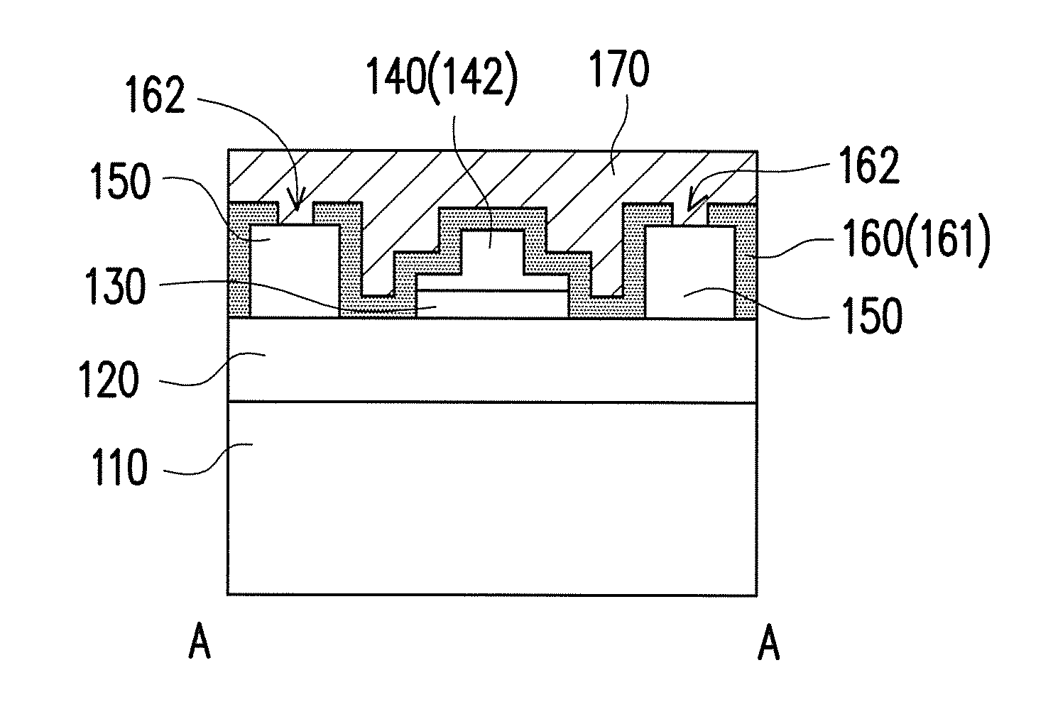
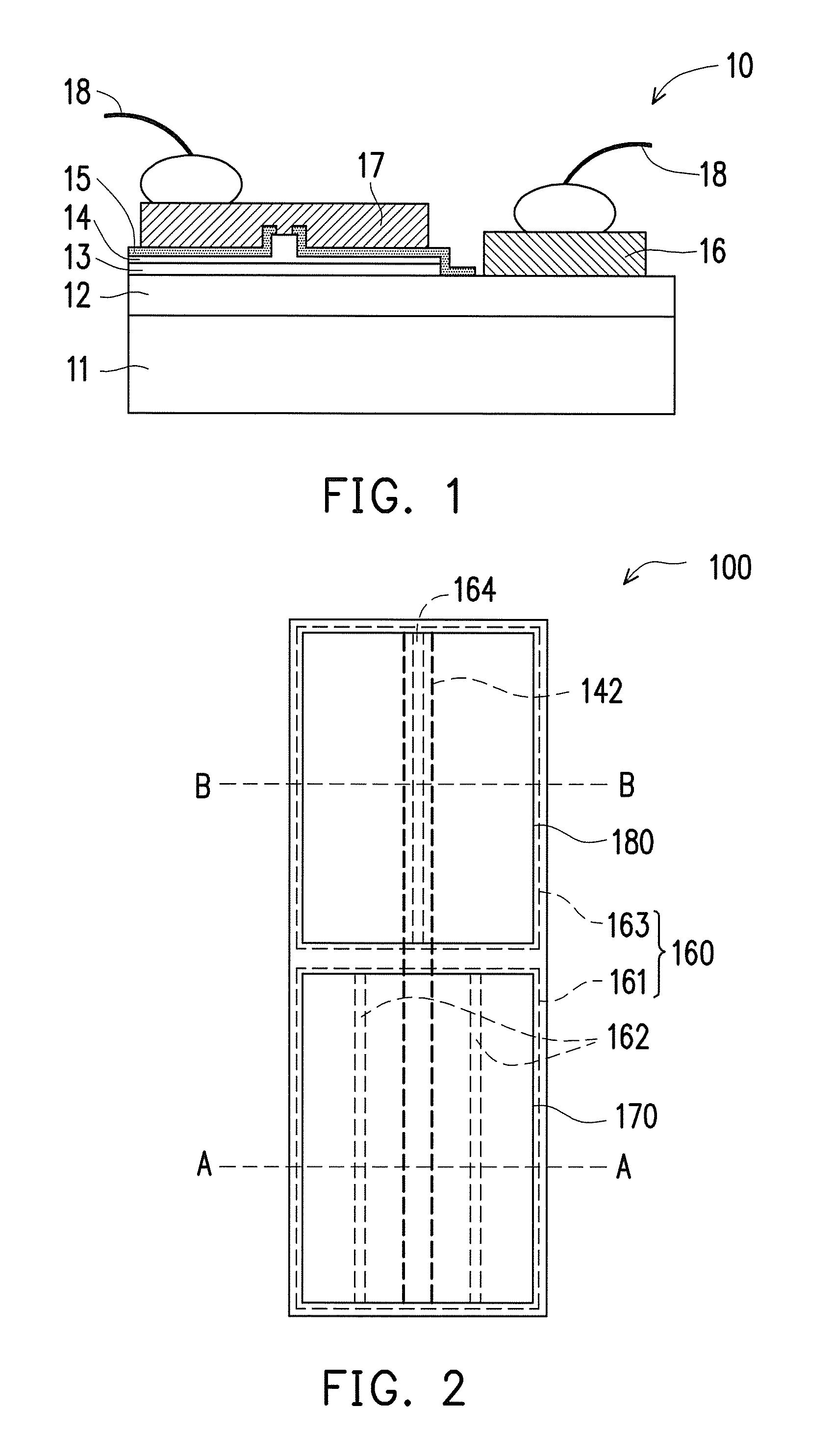
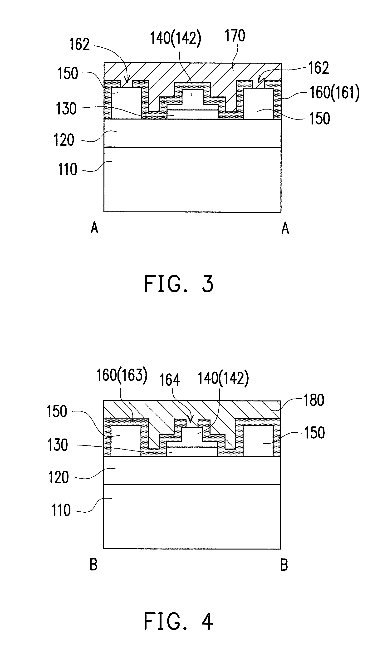
[0035]FIG. 2 is a top schematic view illustrating a flip chip type laser diode according to an embodiment of the invention. FIG. 3 is a cross-sectional schematic view illustrating the flip chip type laser diode shown in FIG. 2 along an A-A line segment. FIG. 4 is a cross-sectional schematic view illustrating the flip chip type laser diode shown in FIG. 2 along a B-B line segment. Referring to FIGS. 2-4, a flip chip type laser diode 100 of this embodiment includes a first substrate 110, a first semiconductor layer 120, an emitting layer 130, a second semiconductor layer 140, at least one current conducting layer 150, a patterned insulating layer 160, a first electrode 170, and a second electrode 180.

[...


PUM


Abstract

A laser diode chip includes a removable substrate, a first semiconductor layer disposed on the removable substrate, an emitting layer disposed on one part of the first semiconductor layer, a second semiconductor layer disposed on the emitting layer and forming a ridge mesa, a current conducting layer disposed on another part of the first semiconductor layer, a patterned insulating layer covering the second semiconductor layer and the current conducting layer and including a first zone and a second zone which respectively expose a part of the current conducting layer and a part of the second semiconductor layer, a first electrode and a second electrode respectively disposed on the first zone and the second zone. A projection of the ridge mesa projected to the removable substrate covers a part of projections of the first electrode and the second electrode projected to the removable substrate.

Description

CROSS-REFERENCE TO RELATED APPLICATION[0001]This application is a continuation-in-part application of and claims the priority benefit of U.S. application Ser. No. 14 / 732,804, filed on Jun. 8, 2015, now allowed, which claims the priority benefit of Taiwan application serial no. 103121394, filed on Jun. 20, 2014. The entirety of each of the above-mentioned patent applications is hereby incorporated by reference herein and made a part of this specification.BACKGROUND OF THE INVENTION[0002]1. Field of the Invention[0003]The invention relates to a laser diode and a laser diode package structure, and particularly relates to a flip chip type laser diode and a flip chip type laser diode package structure.[0004]2. Description of Related Art[0005]FIG. 1 is a cross-sectional schematic view illustrating a conventional laser diode. Referring to FIG. 1, a conventional laser diode 10 includes a substrate 11, a first semiconductor layer 12, an emitting layer 13, a second semiconductor layer 14, a p...

Claims


Application Information

Patent Timeline
Patent Type & Authority Applications(United States)
IPC IPC(8): H01S5/022H01S5/22H01S5/02H01S5/042
CPCH01S5/0224H01S5/0213H01S5/2205H01S5/0425H01L2224/48463H01L2224/49107H01S5/02461H01S5/227H01S5/04257H01S5/0234
Inventor WU, CHIH-LINGLO, YU-YUN
Owner PLAYNITRIDE
Learn More