Light-Emitting Element, Light-Emitting Device, Electronic Device, and Lighting Device

a technology of light-emitting devices and light-emitting elements, which is applied in the direction of organic semiconductor devices, solid-state devices, organic chemistry, etc., can solve problems such as difficulty in realization, and achieve the effect of high emission efficiency and long li

Active Publication Date: 2016-11-17
SEMICON ENERGY LAB CO LTD
View PDF1 Cites 143 Cited by
  • Summary
  • Abstract
  • Description
  • Claims
  • Application Information

AI Technical Summary

Benefits of technology

[0010]An object of one embodiment of the present invention is to provide a novel light-emitting element. Another object of one embodiment of the present invention is to pro...

Problems solved by technology

This feature is difficult to realize with point light sources typified by i...

Method used


Image

  • Light-Emitting Element, Light-Emitting Device, Electronic Device, and Lighting Device
  • Light-Emitting Element, Light-Emitting Device, Electronic Device, and Lighting Device
  • Light-Emitting Element, Light-Emitting Device, Electronic Device, and Lighting Device

Examples


embodiment 1

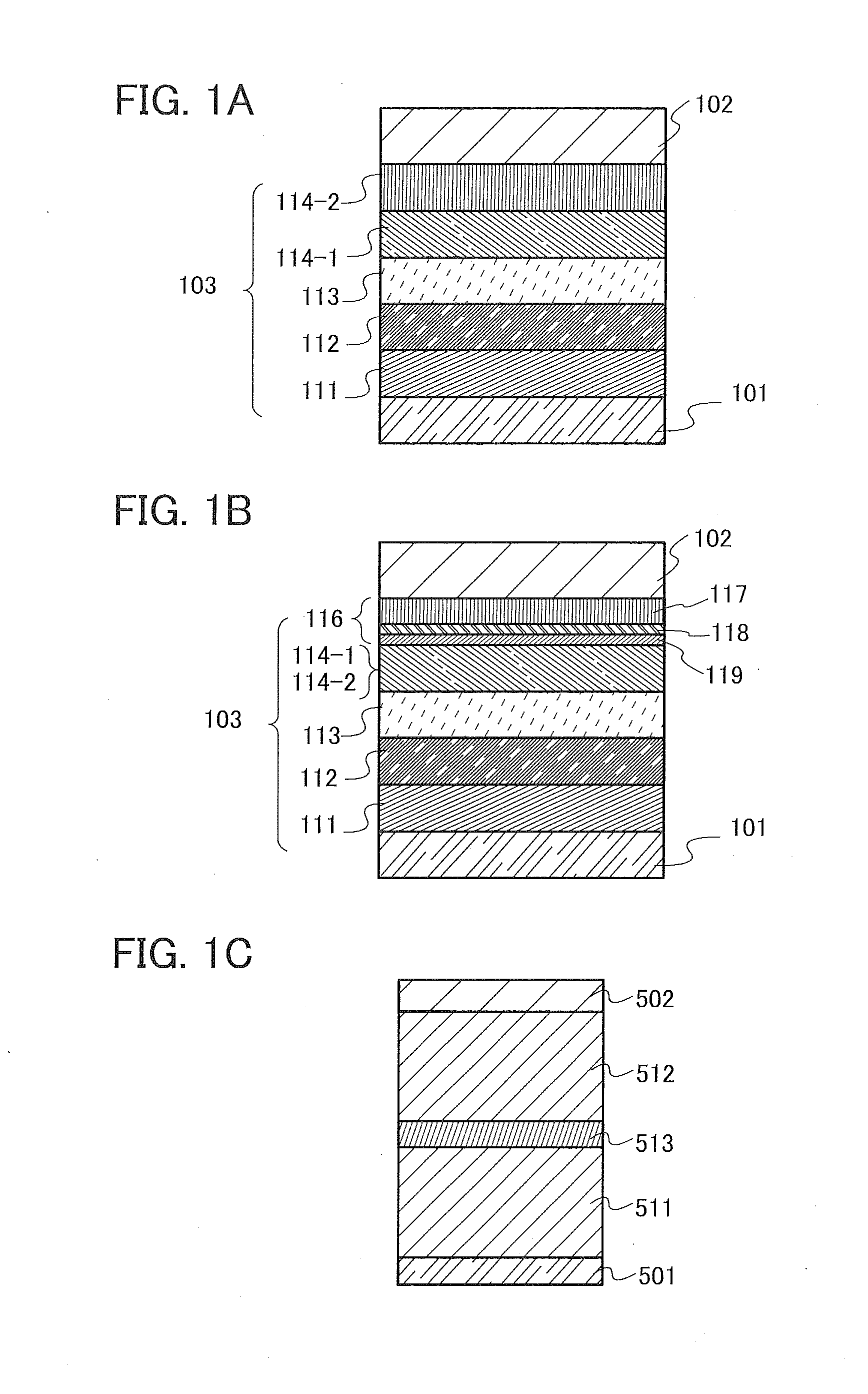
[0073]FIG. 1A illustrates a light-emitting element of one embodiment of the present invention. The light-emitting element of one embodiment of the present invention includes at least an anode 101, a cathode 102, and an EL layer 103. The EL layer 103 includes at least a light-emitting layer 113, a first electron-transport layer 114-1, and a second electron-transport layer 114-2.

[0074]The light-emitting layer 113 contains a host material and a fluorescent substance. By application of voltage to the light-emitting element for letting current flow, light from the fluorescent substance can be obtained.

[0075]The host material is a substance including a condensed aromatic ring skeleton including 3 to 6 rings. A material for the first electron-transport layer 114-1 and a material for the second electron-transport layer 114-2 are substances each including a heteroaromatic ring skeleton. The material for the first electron-transport layer 114-1 is different from the material for the second el...

embodiment 2

[0143]In this embodiment, a light-emitting device including the light-emitting element containing any of the organic compounds described in Embodiment 1 is described.

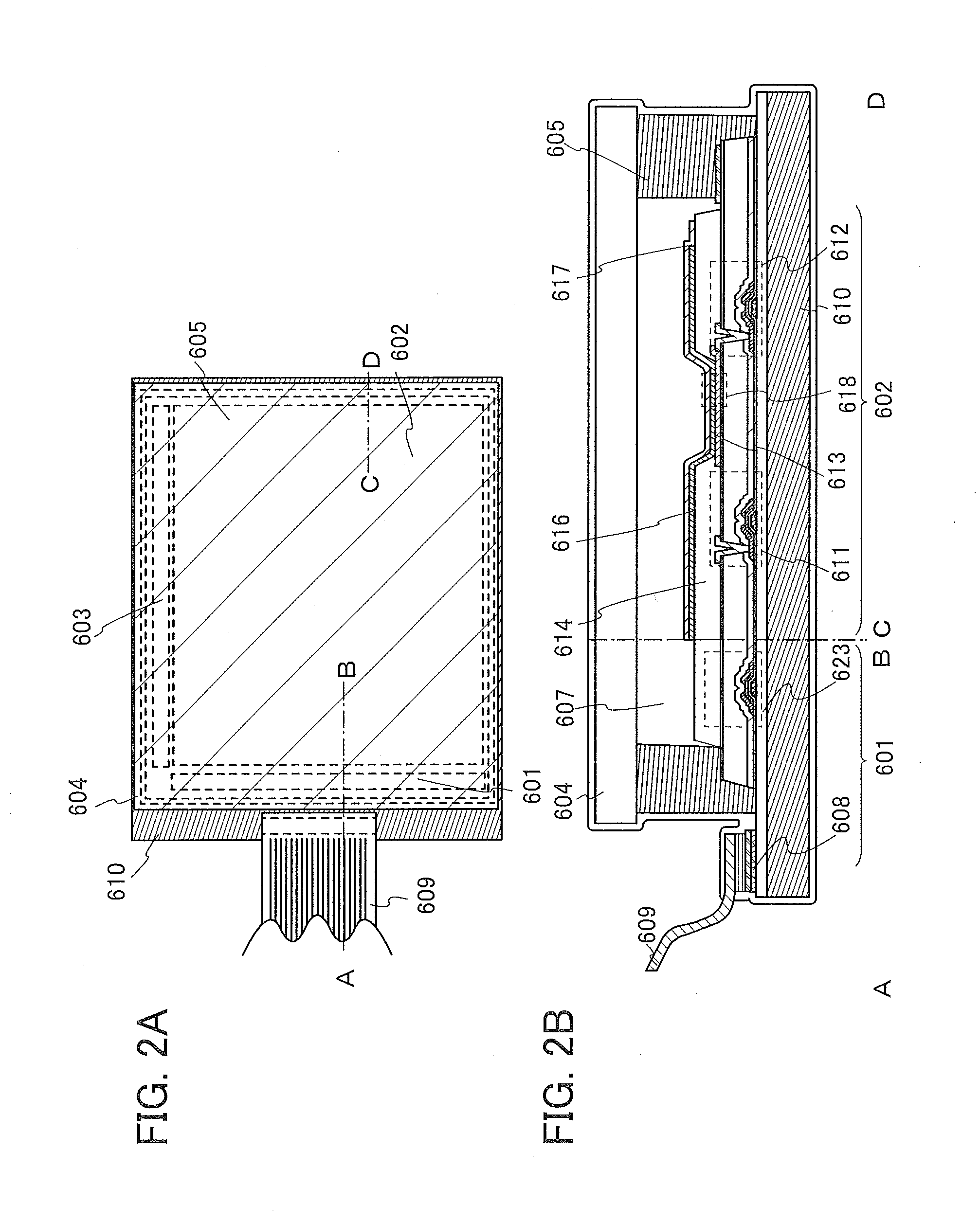
[0144]In this embodiment, the light-emitting device manufactured using the light-emitting element containing any of the organic compounds described in Embodiment 1 is described with reference to FIGS. 2A and 2B. Note that FIG. 2A is a top view of the light-emitting device and FIG. 2B is a cross-sectional view taken along the lines A-B and C-D in FIG. 2A. This light-emitting device includes a driver circuit portion (source line driver circuit) 601, a pixel portion 602, and a driver circuit portion (gate line driver circuit) 603, which are to control light emission of a light-emitting element and illustrated with dotted lines. Reference numeral 604 denotes a sealing substrate; 605, a sealing material; and 607, a space surrounded by the sealing material 605.

[0145]Reference numeral 608 denotes a lead wiring for transmitting...

embodiment 3

[0190]In this embodiment, an example in which the light-emitting element described in Embodiment 1 is used for a lighting device will be described with reference to FIGS. 6A and 6B. FIG. 6B is a top view of the lighting device, and FIG. 6A is a cross-sectional view taken along the line e-f in FIG. 6B.

[0191]In the lighting device in this embodiment, a first electrode 401 is formed over a substrate 400 which is a support and has a light-transmitting property. The first electrode 401 corresponds to the anode 101 in Embodiment 1. When light is extracted through the first electrode 401 side, the first electrode 401 is formed using a material having a light-transmitting property.

[0192]A pad 412 for applying voltage to a second electrode 404 is provided over the substrate 400.

[0193]An EL layer 403 is formed over the first electrode 401. The structure of the EL layer 403 corresponds to, for example, the structure of the EL layer 103 in Embodiment 1, or the structure in which the light-emitt...


PUM

PropertyMeasurementUnit
Currentaaaaaaaaaa
Currentaaaaaaaaaa
Currentaaaaaaaaaa

Abstract

Provided is a novel light-emitting element, a light-emitting element with a long lifetime, or a light-emitting element with high emission efficiency. The light-emitting element includes an EL layer between a pair of electrodes. The EL layer includes at least a light-emitting layer containing a fluorescent substance and a host material, a first electron-transport layer containing a first electron-transport material, and a second electron-transport layer containing a second electron-transport material, which are in contact with each other and in this order. The LUMO level of each of the host material and the second electron-transport material is higher than the LUMO level of the first electron-transport material.

Description

BACKGROUND OF THE INVENTION[0001]1. Field of the Invention[0002]One embodiment of the present invention relates to a light-emitting element, a display module, a lighting module, a display device, a light-emitting device, an electronic device, and a lighting device in which the organic compound is used. Note that one embodiment of the present invention is not limited to the above technical field. The technical field of one embodiment of the invention disclosed in this specification and the like relates to an object, a method, or a manufacturing method. In addition, one embodiment of the present invention relates to a process, a machine, manufacture, or a composition of matter. Specifically, examples of the technical field of one embodiment of the present invention disclosed in this specification include a semiconductor device, a display device, a liquid crystal display device, a light-emitting device, a lighting device, a power storage device, a memory device, an imaging device, a me...

Claims


Application Information

Patent Timeline
IPC IPC(8): H01L51/00
CPCH01L51/0072H01L51/5012H01L51/0061H01L51/0052H01L51/0058H01L51/0054H01L51/0074H01L51/0067H01L51/0065H01L51/0056H01L51/0055H01L51/0071H01L51/0073H01L51/008H01L51/5004H01L2251/552H01L51/508H01L51/006H10K85/615H10K85/654H10K50/11H10K2101/40H10K85/6572H10K50/155H10K50/166H10K50/841H10K2101/30C07C15/28H10K59/00H10K59/12H10K85/111H10K50/12H10K50/17
Inventor SEO, SATOSHISUZUKI, TSUNENORIHASHIMOTO, NAOAKI
Owner SEMICON ENERGY LAB CO LTD
Why Eureka
Try Eureka