Unlock instant, AI-driven research and patent intelligence for your innovation.

Substrate and manufacturing method thereof, and display device

a technology of substrate and manufacturing method, applied in the field of substrate, can solve the problems of large delay of gate driving signal or source driving signal, rendering gray scale display abnormal, etc., and achieve the effect of reducing the resistance of gate lines

Active Publication Date: 2016-11-24
BOE TECH GRP CO LTD
View PDF5 Cites 14 Cited by
  • Summary
  • Abstract
  • Description
  • Claims
  • Application Information

AI Technical Summary

Benefits of technology

The present invention provides a substrate and manufacturing method for reducing resistance in a display device. This is achieved by adding first auxiliary gate or data lines that are connected to the main lines through via holes. This reduces signal delay caused by resistance in the gate or data lines, resulting in improved display performance.

Problems solved by technology

Whereas the gate driving circuit needs to input the gate driving signal into the pixel unit through the gate line, the source driving circuit also needs to input the converted source driving signal into the pixel unit through the data line, hence, the larger and larger resistance in the gate line or the data line will result in larger and larger delay of the gate driving signal or the source driving signal, thereby rendering gray scale display abnormal.

Method used


Image

  • Substrate and manufacturing method thereof, and display device
  • Substrate and manufacturing method thereof, and display device
  • Substrate and manufacturing method thereof, and display device

Examples


Embodiment Construction

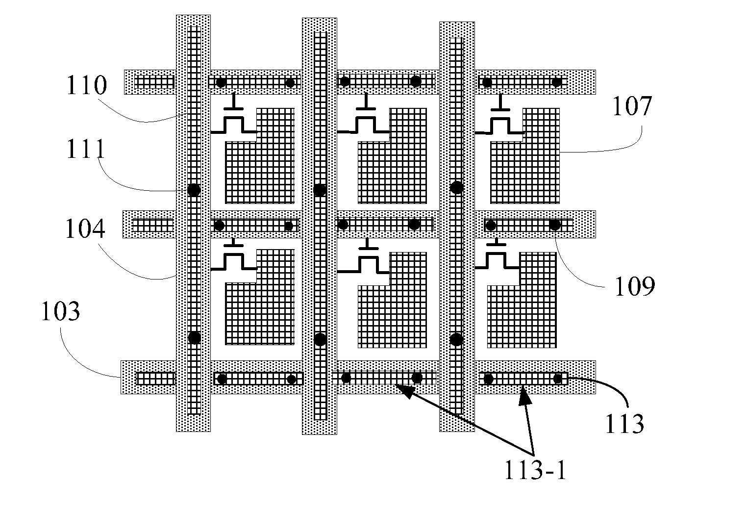
[0047]Next, the substrate and the manufacturing method thereof, as well as the display device provided by the embodiments of the present invention will be described in detail with reference to the drawings, wherein the same reference sign is used to indicate the same component in the text. In the following description, large amount of details are provided for the convenience of explanation, so as to provide a comprehensive understanding to one or more embodiments. However, it is obvious that the embodiments can also be carried out not using these details. In other examples, the well known structure and device are shown in the form of block diagrams, for the convenience of describing one or more embodiments.

[0048]The expressions “upper”, “lower” in the embodiments of the present invention depend on the sequence when manufacturing the substrate, for example, the upper pattern refers to a pattern formed later, the lower pattern refers to a pattern formed earlier.

[0049]One embodiment of...


PUM

PropertyMeasurementUnit
transparent conductiveaaaaaaaaaa
areasaaaaaaaaaa
transparentaaaaaaaaaa

Abstract

The embodiments of the present invention provide a substrate and a manufacturing method thereof, as well as a display device. The substrate comprises: a base substrate, a plurality of gate lines arranged in parallel, a first insulating layer that covers the gate lines, a plurality of data lines located on the first insulating layer and perpendicular to the gate lines, a second insulating layer that covers the data lines, and pixel electrodes of sub-pixel areas enclosed by the data lines and the gate lines; polarizing films that cover the pixel electrodes; and first auxiliary gate lines arranged on the second insulating layer and parallel to the gate lines, at least two portions on each of the first auxiliary gate lines being electrically connected with at least two corresponding portions on the gate line through via holes that penetrate the first insulating layer and the second insulating layer, the first auxiliary gate lines and the polarizing films are formed by performing a same patterning process to a same layer of transparent conductive material. The embodiments of the present invention can reduce signal delay in a display device, and can be used for manufacture of a display.

Description

FIELD OF THE INVENTION[0001]The present invention relates to the field of display manufacturing, particularly to a substrate and a manufacturing method thereof, as well as a display device.BACKGROUND OF THE INVENTION[0002]Liquid crystal display (LCD) has the advantages of light weight, small thickness and low power consumption etc.; it has been widely used in electronic products such as television, mobile phone, display and so on. A liquid crystal display is constituted by pixel matrix in both horizontal and vertical directions. When the liquid crystal display performs display, a driving circuit outputs a driving signal to scan the respective pixel units row by row. The driving circuit of the liquid crystal display mainly comprises a gate driving circuit and a source driving circuit, the source driving circuit latches the inputted display data and clock signals in sequence at regular time, converts them into source driving signals and inputs them into the data lines of the liquid cr...

Claims


Application Information

Patent Timeline
Patent Type & Authority Applications(United States)
IPC IPC(8): G02F1/1362G02F1/1343G02F1/1335H01L27/12G02F1/1333
CPCG02F1/136286H01L27/124H01L27/1259G02F1/133345G02F1/133528G02F2001/136295G02F1/13439G02F2001/13629G02F2201/123G02F2001/133548G02F1/136227H01L21/82H01L2924/0002G02F1/133548G02F1/13629H01L2924/00H01L23/481H01L21/768H01L21/84G02F1/136295H01L23/50
Inventor ZHANG, XIANGYANWU, YANBINGLI, WENBOLI, PANJIA, QIAN
Owner BOE TECH GRP CO LTD