Mutual capacitance one glass solution touch panel and manufacture method thereof

a technology of capacitance and touch panel, applied in the field of touch screen technology, can solve the problems of reducing affecting the operation of touch control, so as to reduce the resistance of transmission signals in the electrode pattern and raise the sensitivity of touch control

Active Publication Date: 2016-11-24
TCL CHINA STAR OPTOELECTRONICS TECH CO LTD
View PDF8 Cites 9 Cited by
  • Summary
  • Abstract
  • Description
  • Claims
  • Application Information

AI Technical Summary

Benefits of technology

[0022]With the aforesaid technical solutions, the benefits of the present invention are: the embodiment of the present invention forms the first through hole and the second through hole at an isolation layer, the first sub electrode pattern is electrically connected to the fourth sub electrode pattern via the first through hole, and the third sub electrode pattern is electrically connected to the second sub electrode pattern via the second through hole as touch control test is performed to the touch panel. The formations of the first through hole and the fourth sub electrode pattern are equivalent to adding a wiring layer of transmitting signals for the first sub electrode pattern. The formations of the second through hole and the second sub electrode pattern are equivalent to adding a wiring layer of transmitting signals for the third sub electrode pattern. Accordingly, the wire resistance of the transmission signals in the electrode patterns can be reduced to raise the touch control sensitivity.

Problems solved by technology

The resistance of the ITO transparent conductive material is too big which can extremely easily make the transmitting signals of the sensing lines and the emitting lines seriously decayed and distorted.
Consequently, it leads to tremendous decrease of the touch control sensitivity.
However, the increase of the current will certainly add power consumption.

Method used


Image

  • Mutual capacitance one glass solution touch panel and manufacture method thereof
  • Mutual capacitance one glass solution touch panel and manufacture method thereof
  • Mutual capacitance one glass solution touch panel and manufacture method thereof

Examples


Embodiment Construction

[0028]Embodiments of the present invention are described in detail with the technical matters, structural features, achieved objects, and effects with reference to the accompanying drawings as follows. It is clear that the described embodiments are merely part of embodiments of the present invention, but not all embodiments. Based on the embodiments of the present invention, all other embodiments to those of ordinary skill in the premise of no creative efforts obtained, should be considered within the scope of protection of the present invention.

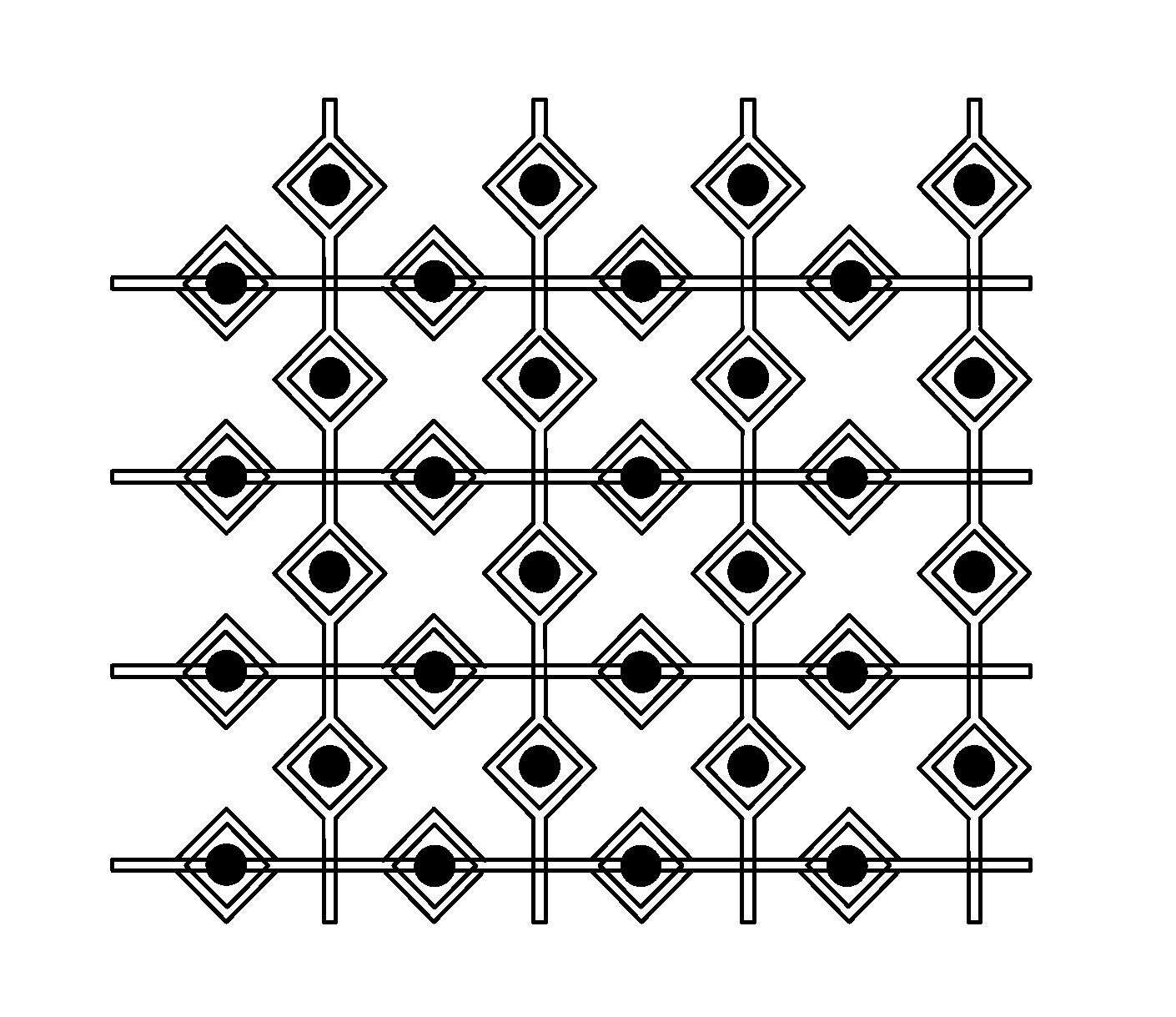
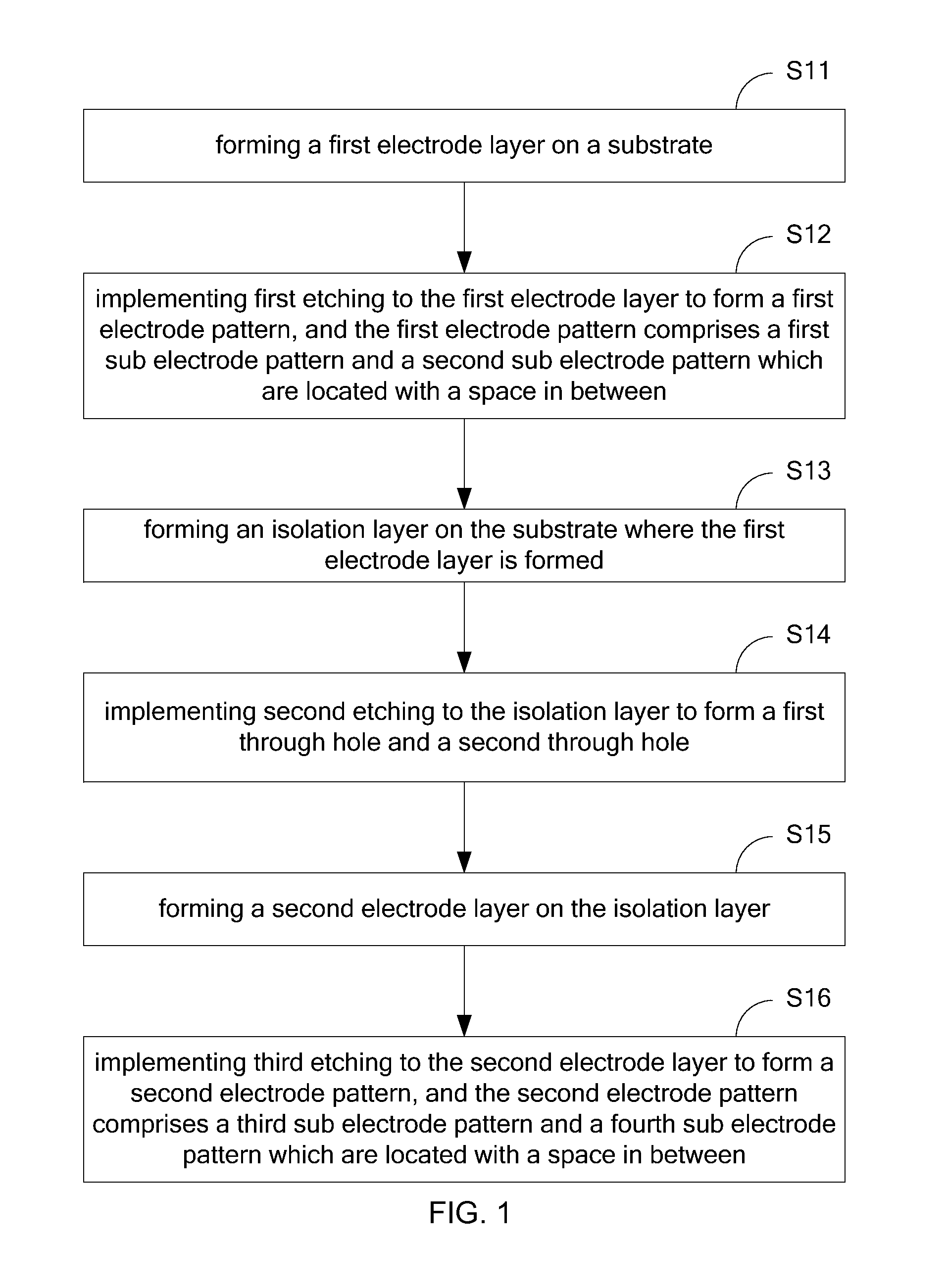
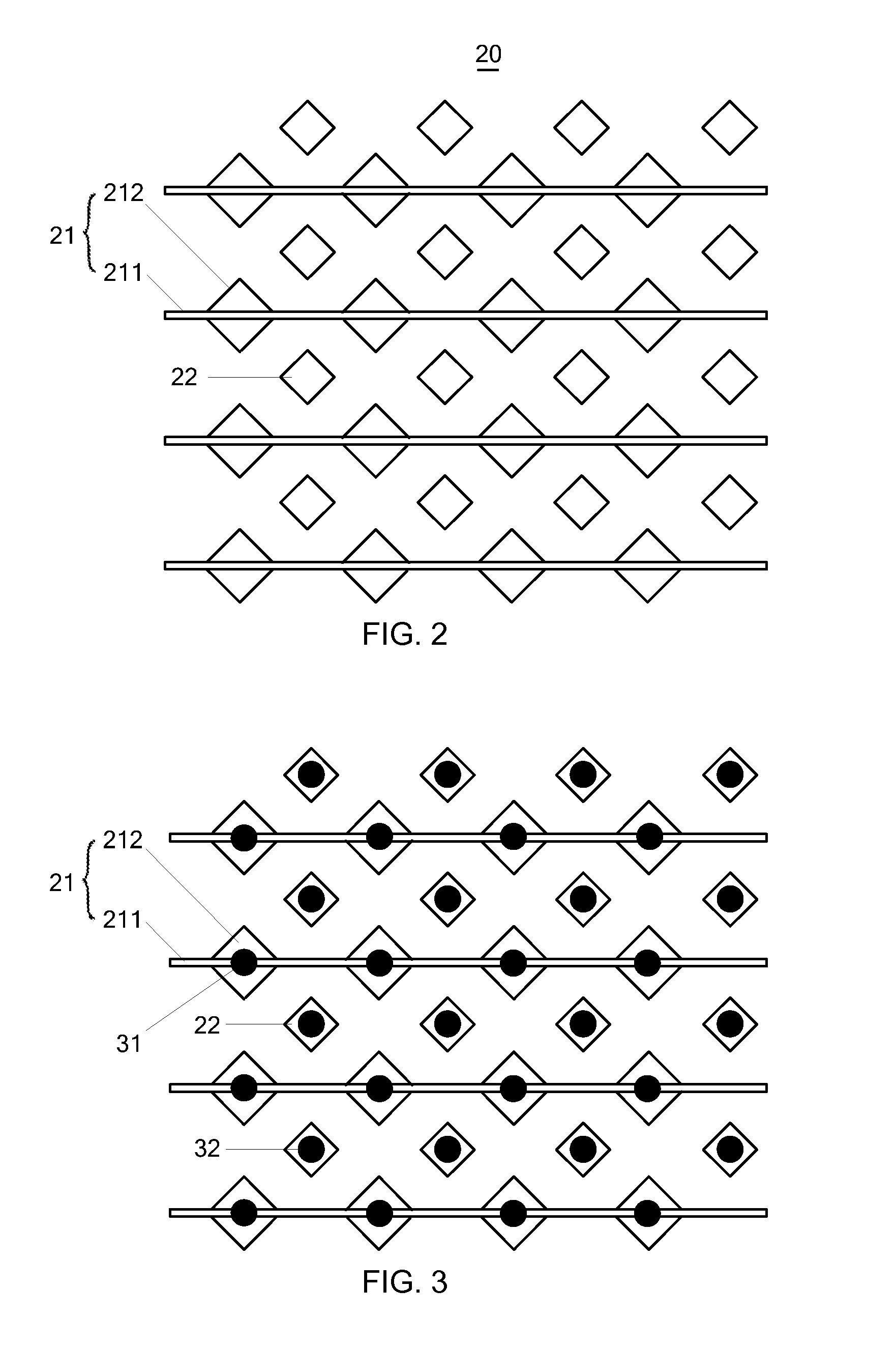
[0029]FIG. 1 is a flowchart of a manufacture method of a touch panel according to the preferred embodiment of the present invention. Please refer to FIG. 1. The manufacture method of the embodiment comprises:

[0030]Step S11: forming a first electrode layer on a substrate.

[0031]The substrate can be a transparent glass substrate, a transparent plastic substrate or a transparent flexible substrate. The first electrode layer can be an Indium Tin ...


PUM


Abstract

The present invention provides a mutual capacitance one glass solution touch panel and a manufacture method thereof. A first through hole and a second through hole are formed at an isolation layer of the touch panel. A first sub electrode pattern of the touch panel is electrically connected to a fourth sub electrode pattern of the touch panel via the first through hole, and a third sub electrode pattern of the touch panel is electrically connected to a second sub electrode pattern of the touch panel via the second through hole as touch control test is performed. According to the aforesaid arrangement, the present invention is capable of reducing the wire resistance of the transmission signals in the electrode patterns to raise the touch control sensitivity.

Description

FIELD OF THE INVENTION[0001]The present invention relates to a touch screen technology field, and more particularly to a mutual capacitance one glass solution touch panel and a manufacture method thereof.BACKGROUND OF THE INVENTION[0002]With the development of touch screen technology and higher demands of the market to the thin touch screen, the mutual capacitance one glass solution touch panel possesses advantages of strong anti-interference capability, high sensitivity, distinguishable multi-touch, et cetera has become the major lead of the touch screen technology field.[0003]The mutual capacitance one glass solution touch panel is also so called unified mutual capacitance touch panel. Fringing field capacitors can be formed at the fringes of different electrode patterns of the only glass substrate. When the touch control is functioning, the fringing field capacitor can change. By detecting the transmitting signals of the sensing lines and the emitting lines, the coordinates of th...

Claims


Application Information

Patent Timeline
Patent Type & Authority Applications(United States)
IPC IPC(8): G06F3/044
CPCG06F3/044G06F2203/04103G06F2203/04111G06F3/0445G06F3/0446G02F1/13338
Inventor XU, XIANGYANG
Owner TCL CHINA STAR OPTOELECTRONICS TECH CO LTD
Why Eureka
Try Eureka