Semiconductor device

Active Publication Date: 2016-11-24
FUJI ELECTRIC CO LTD
View PDF2 Cites 20 Cited by
  • Summary
  • Abstract
  • Description
  • Claims
  • Application Information

AI Technical Summary

Benefits of technology

[0016]According to the semiconductor device of the present invention, although downsizing and thinning of a cooler is disadvantageous in terms of pressure loss, turbulence in the flow of a cooling liquid is maximally reduced so that pressure loss is reduced, and the connection portions for connecting pipes of the inlet portion and the outle

Problems solved by technology

Power semiconductor elements generate a large amount of heat when controlling high current.
However, in a case where the flow rate of a cooling liquid into a cooler is increased or fins are formed into a shape having high heat transfer rate, disadvantages tend to occur such as increase in p

Method used


Image

  • Semiconductor device
  • Semiconductor device
  • Semiconductor device

Examples


Example

First Embodiment

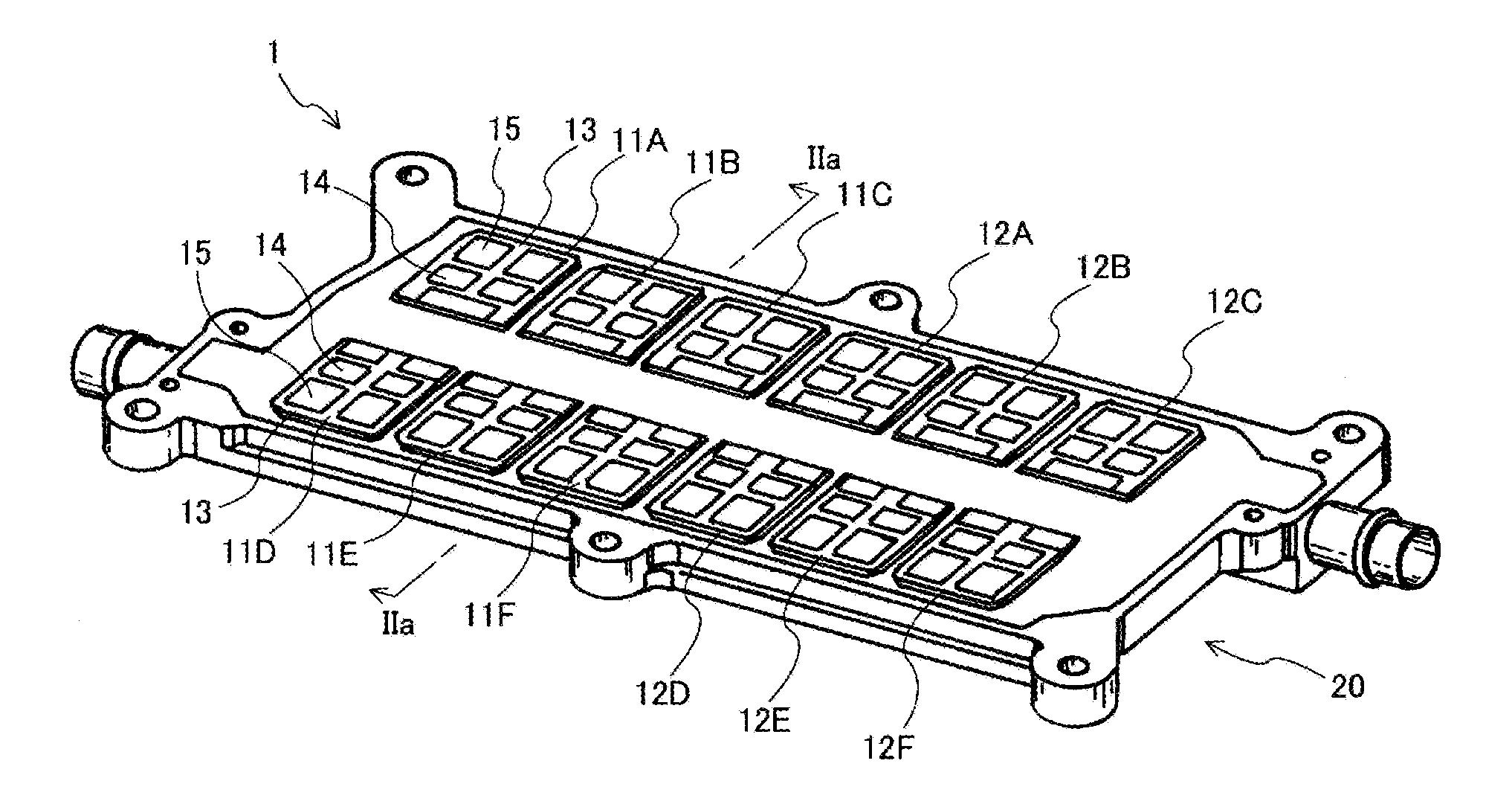
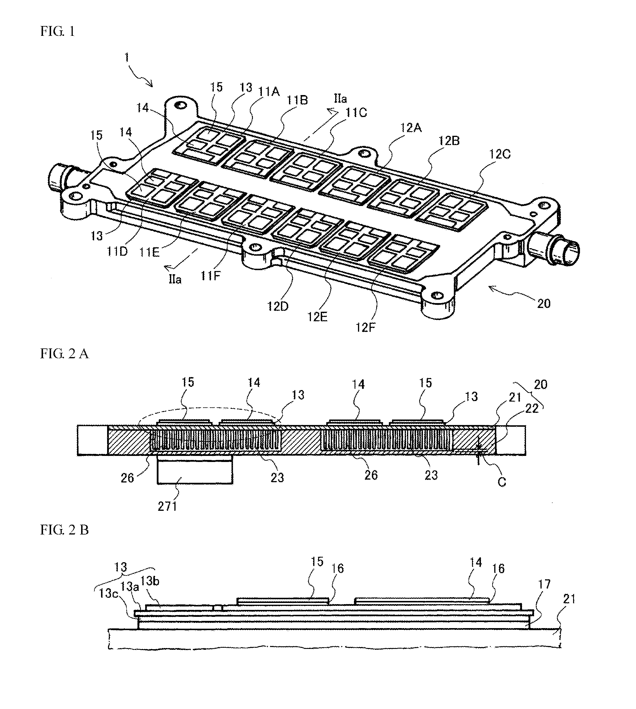
[0043]FIG. 1 is a perspective diagram depicting an appearance of one example of a semiconductor module that is one embodiment of the semiconductor device of the invention. FIG. 2 A is a schematic diagram depicting the semiconductor module of FIG. 1 by a section as viewed from an arrow direction of line IIa-IIa, and FIG. 2 B is a schematic diagram of an enlarged portion of FIG. 2 A.

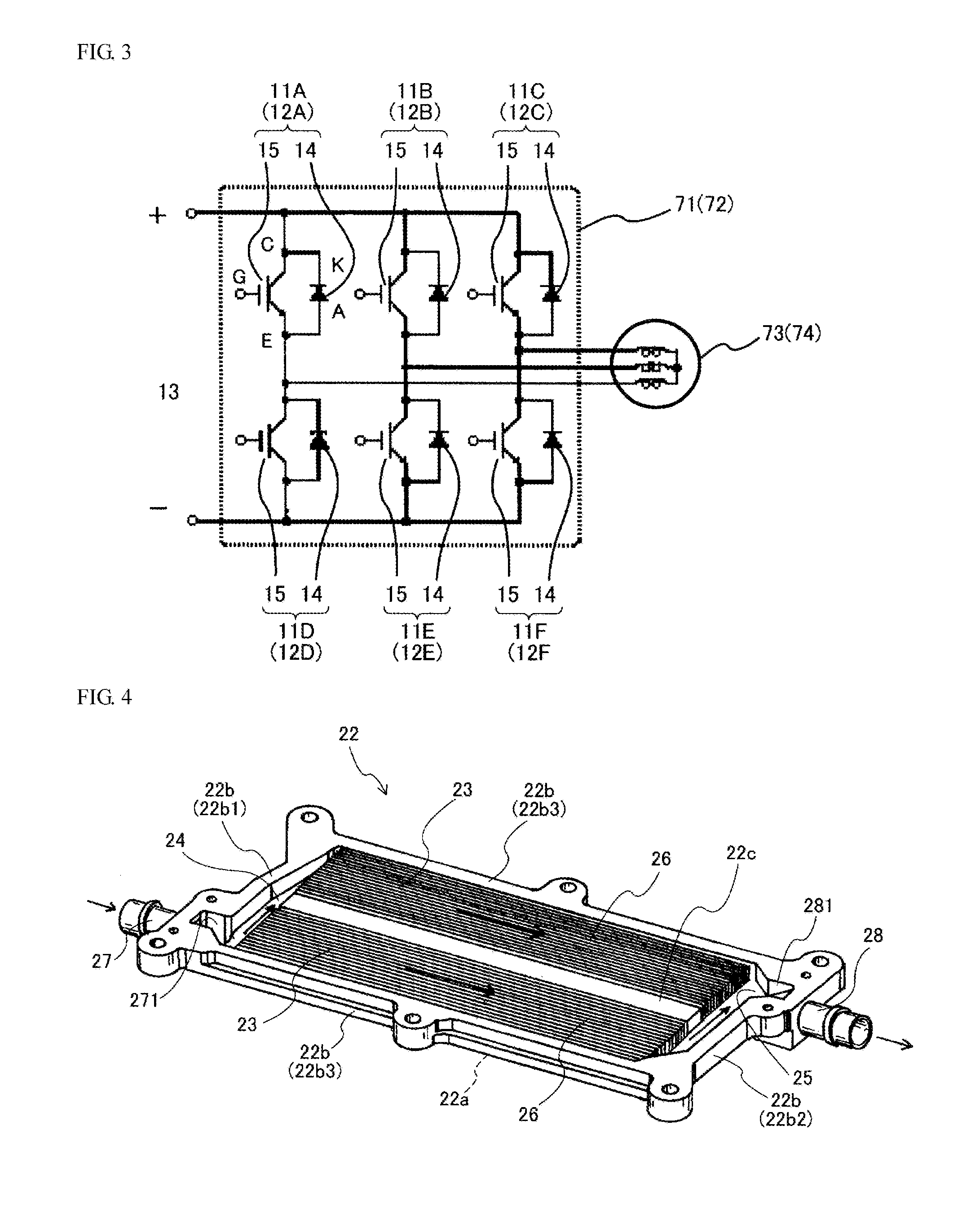
[0044]A semiconductor module 1 includes a plurality of circuit element units 11A to 11F and 12A to 12F and a cooler 20 to which the circuit element units 11A to 11F and 12A to 12F are connected, as depicted in FIG. 1 and FIGS. 2 A and 2 B.

[0045]The respective circuit element units 11A to 11F and 12A to 12F all have a structure, for example, in which two kinds of semiconductor elements 14 and 15 are mounted two by two, four in total on a circuit substrate 13. The circuit substrate 13 has a structure in which conductor layers 13b and 13c are formed on both surfaces of an insulation plate 13a,...

Example

Second Embodiment

[0083]Next, a semiconductor device of a second embodiment of the present invention will be described. The semiconductor device of the present embodiment has the same structure as the semiconductor device of the first embodiment, except for the shapes of the connection portion 271 and the connection portion 281 in the semiconductor device of the first embodiment. Accordingly, the shapes of the connection portion 271 and the connection portion 281 will be described below. Additionally, the same reference symbols are given to members and parts thereof having the same functions as the members and parts thereof given in FIG. 5 and FIG. 7 describing the semiconductor device of the first embodiment, and thus duplicated descriptions thereof are omitted below.

[0084]FIG. 9 depicts an enlarged view of the connection portion 271 of the semiconductor device of the second embodiment. The first inclined surface 271a of the connection portion 271 of FIG. 9 has a shape extending to ...

Example

Third Embodiment

[0087]Next, a semiconductor device of a third embodiment of the present invention will be described. The semiconductor device of the present embodiment has the same structure as the semiconductor device of the first embodiment, except for the structure of the cooling flow path 26 in the semiconductor device of the first embodiment. Accordingly, the structure of the cooling flow path 26 in the present embodiment will be described below.

[0088]FIG. 10 depicts a plan view depicting an inner structure of the cooler 20 in the semiconductor device of the present embodiment. FIG. 10 is a drawing corresponding to FIG. 5 depicting the cooler of the first embodiment, and the same members as those depicted in FIG. 5 are denoted by the same reference symbols. Thus, duplicated descriptions of the respective members are omitted.

[0089]The case 22 depicted in FIG. 10 is different from the case 22 of the semiconductor device of the first embodiment depicted in FIG. 5 in terms of the p...


PUM


Abstract

A cooler 20 of a semiconductor device includes an inlet portion 27 and an outlet portion 28 for a cooling liquid, an inlet path 24, an outlet path 25, and a cooling flow path 26. The inlet path 24 and the outlet path 25 have asymmetrical planar shapes. A connection portion 271 between the inlet path 24 and the inlet portion 27 is opposed to the cooling flow path 26 of a part immediately below plural circuit substrates 13 arranged on the cooler 20. A connection portion 281 between the outlet path 25 and the outlet portion 28 is opposed to the cooling flow path 26 of a part immediately below plural circuit substrates 13 arranged on the cooler 20.

Description

CROSS-REFERENCE TO RELATED APPLICATIONS[0001]This application is a continuation of PCT Application No. PCT / JP2015 / 072005, which claims priority to Japanese Patent Application No. 2014-160520, filed Aug. 6, 2014. The contents of these applications are incorporated herein by reference in their entirety.TECHNICAL FIELD[0002]The present invention relates to a semiconductor device including a cooler that circulates and distributes a cooling liquid for cooling semiconductor elements.BACKGROUND ART[0003]Machines using motors, as typified by hybrid automobiles, electric automobiles, and the like, utilize electric power conversion devices for saving energy. For the electric power conversion devices, semiconductor modules are widely utilized. The semiconductor modules include power semiconductor elements to control high current.[0004]Power semiconductor elements generate a large amount of heat when controlling high current. Additionally, downsizing and weight reduction of semiconductor module...

Claims


Application Information

Patent Timeline
IPC IPC(8): H01L23/473H01L23/367H01L25/18
CPCH01L23/473H01L23/3672H01L23/3675H01L25/18H01L24/29H01L24/32H01L24/45H01L24/48H01L24/73H01L25/072H01L2224/291H01L2224/32225H01L2224/45655H01L2224/48227H01L2224/73265H01L2924/13055H05K7/20927H01L2924/014H01L2924/00014H01L2924/00012
Inventor GOHARA, HIROMICHIMOROZUMI, AKIRAICHIMURA, TAKESHI
Owner FUJI ELECTRIC CO LTD
Why Eureka
Try Eureka