Low temperature poly silicon thin film transistors (ltps tfts) and TFT substrates

a thin film transistor and low temperature technology, applied in the field of liquid crystal display technology, can solve the problems of limited masking effect of light shielding layer and low feed through voltage, and achieve the effect of enhancing tft performance and reducing feed through voltag

Active Publication Date: 2016-11-24
TCL CHINA STAR OPTOELECTRONICS TECH CO LTD
View PDF4 Cites 0 Cited by
  • Summary
  • Abstract
  • Description
  • Claims
  • Application Information

AI Technical Summary

Benefits of technology

[0020]In view of the above, the LTPS TFT includes: a substrate; a first gate arranged on the substrate; a polysilicon layer arranged on the substrates, and the polysilicon layer covers the first gate, wherein the polysilicon layer comprises a source area, a drain area, and a trench area formed between the source area and the drain area; a second gate arranged on the polysilicon layer; wherein when the LTPS TFT has been driven, the first gate and the second gate are respectively applied with a first voltage and a second voltage, and a polarity of the first voltage is opposite to the polarity of the second voltage. In this way, the feed through voltage may be reduced such that the TFT performance is enhanced.

Problems solved by technology

However, the masking effect of the light shielding layer is limited, and may cause the feed through voltage of the gate when the light shielding layer and other conductive layers have generated parasitic capacitance.

Method used


Image

  • Low temperature poly silicon thin film transistors (ltps tfts) and TFT substrates
  • Low temperature poly silicon thin film transistors (ltps tfts) and TFT substrates
  • Low temperature poly silicon thin film transistors (ltps tfts) and TFT substrates

Examples


Embodiment Construction

[0026]Embodiments of the invention will now be described more fully hereinafter with reference to the accompanying drawings, in which embodiments of the invention are shown.

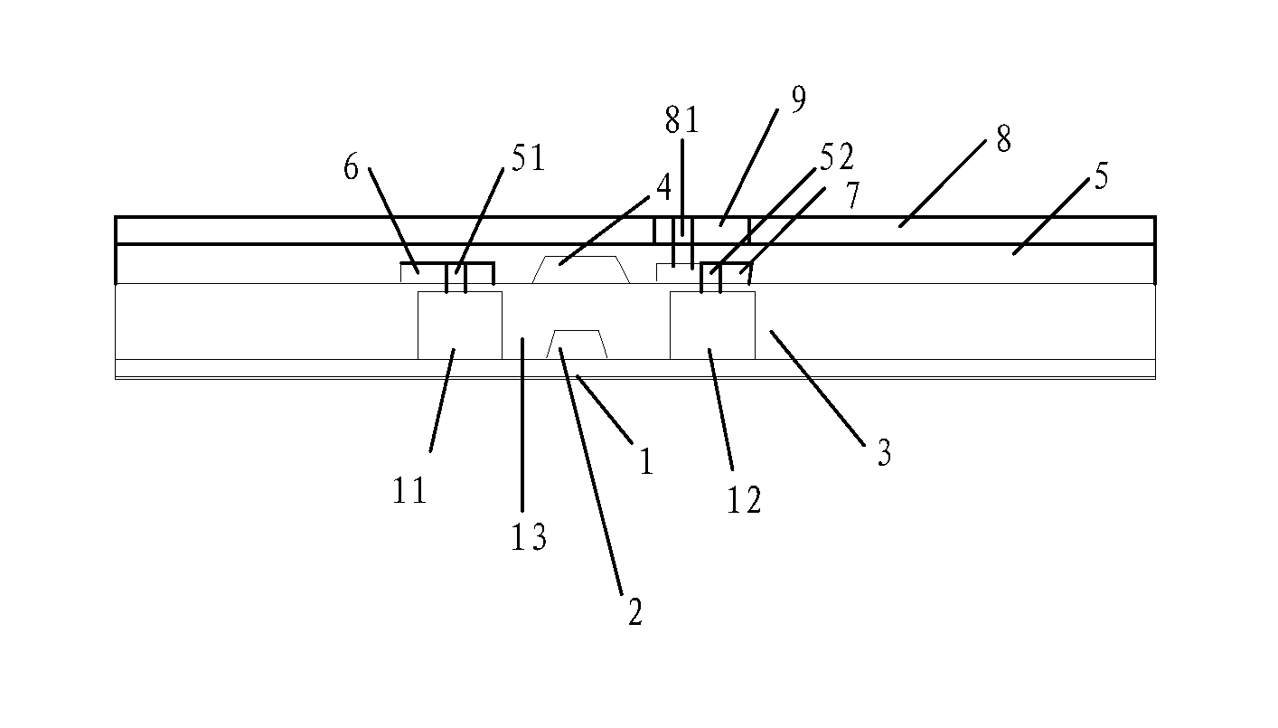
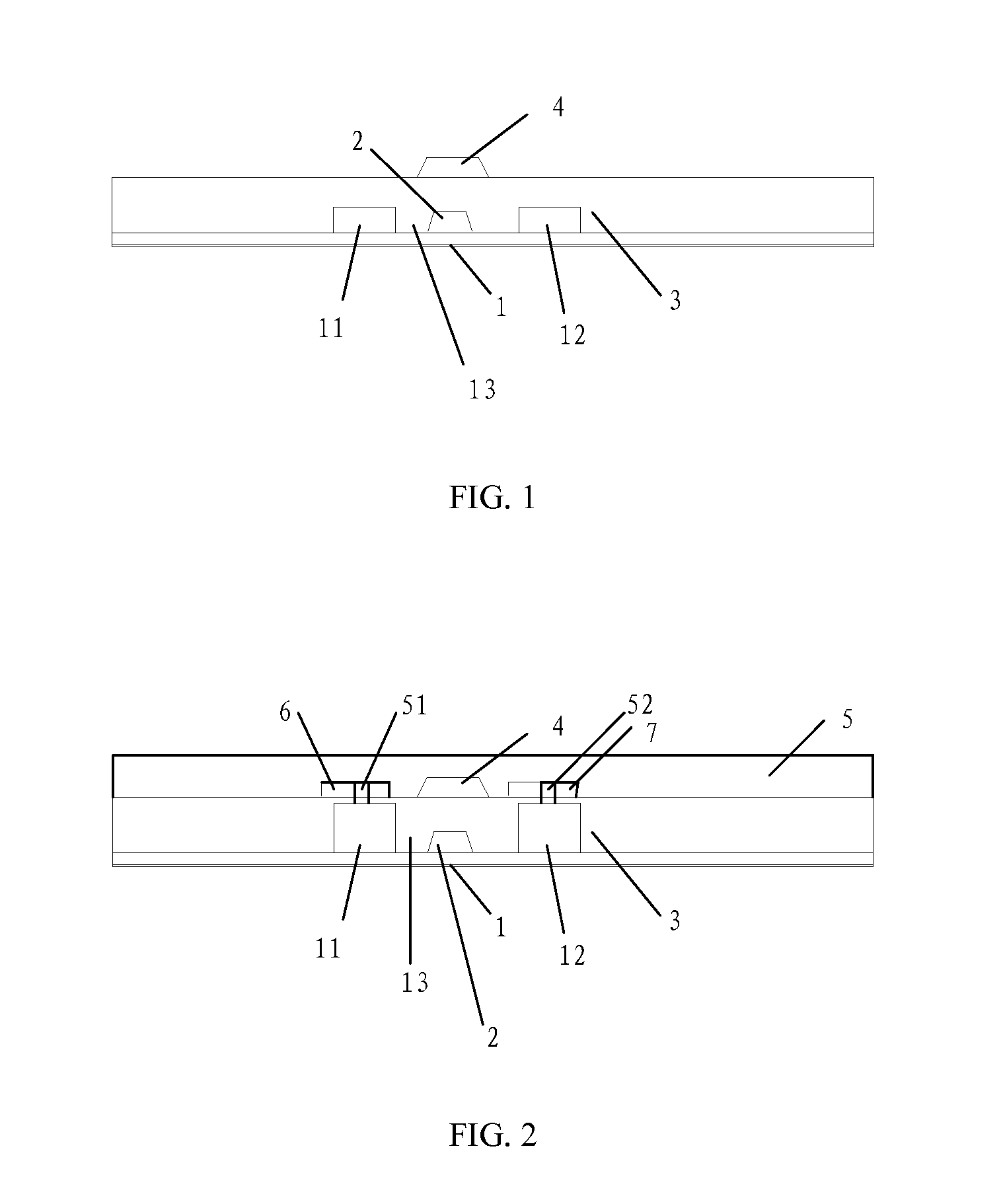
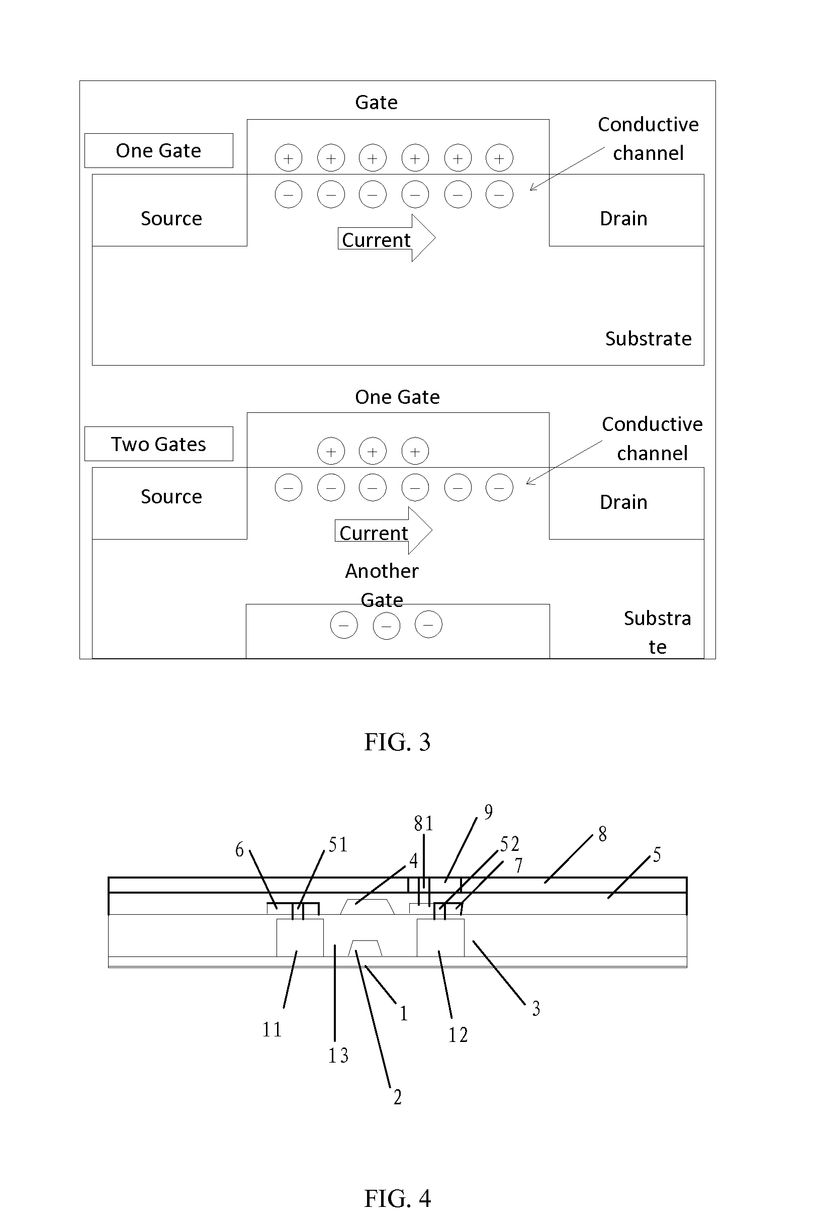
[0027]FIG. 1 is a schematic view of the LTPS TFT in accordance with one embodiment. The LTPS TFT includes a substrate 1, a first gate 2, a polysilicon layer 3, and a second gate 4. The first gate 2 is arranged on the substrate 1. The polysilicon layer 3 is arranged on the substrate 1, and the polysilicon layer 3 covers the first gate 2. The polysilicon layer 3 includes a source area 11, a drain area 12, and a trench area 13 formed between the source area 11 and the drain area 12. The second gate 4 is formed on the polysilicon layer 3.

[0028]When the LTPS TFT has been driven, the first gate 2 and the second gate 4 are respectively applied with a first voltage and a second voltage, and the polarity of the first voltage is opposite to that of the second voltage.

[0029]As the LTPS TFT includes the first gate 2 and the ...


PUM


Abstract

A LTPS TFT and a TFT substrate are disclosed. The LTPS TFT includes: a substrate; a first gate arranged on the substrate; a polysilicon layer arranged on the substrates, and the polysilicon layer covers the first gate, wherein the polysilicon layer comprises a source area, a drain area, and a trench area formed between the source area and the drain area; a second gate arranged on the polysilicon layer; wherein when the LTPS TFT has been driven, the first gate and the second gate are respectively applied with a first voltage and a second voltage, and a polarity of the first voltage is opposite to the polarity of the second voltage. In this way, the feed through voltage may be reduced such that the TFT performance is enhanced.

Description

BACKGROUND OF THE INVENTION[0001]1. Field of the Invention[0002]The present disclosure relates to liquid crystal display technology, and more particularly to LTPS TFTs and TFT substrates.[0003]2. Discussion of the Related Art[0004]LTPS TFT Liquid Crystal Displays (LCDs) are characterized by attributes such as high resolution rate, short response time, high brightness, and high aperture rate. In addition, silicon crystalline arrangement of the LTPS TFT has a specific sequence and mobility of the electrodes is relatively high. External driving circuit may be manufactured on the glass substrate so as to save the space and to reduce the cost of the driving IC.[0005]With respect to conventional LTPS TFT, in order to prevent the leakage current caused by the photo current within the conductive channel, usually, a metallic layer is plated above the glass substrate to operate as a light shielding layer.[0006]However, the masking effect of the light shielding layer is limited, and may cause ...

Claims


Application Information

Patent Timeline
Patent Type & Authority Applications(United States)
IPC IPC(8): H01L29/786H01L29/423G09G3/36H01L27/12
CPCH01L29/78678H01L29/78648H01L27/1222H01L29/42356H01L29/42384H01L27/124G09G2300/0876G09G3/3614G09G3/3677G09G2320/0214G09G2310/08G09G2310/0205G09G3/3696H01L27/1214H01L29/78672G09G2300/0417H01L29/78618H01L29/78633H01L29/78696H01L29/786
Inventor CHEN, CHIU-CHUAN
Owner TCL CHINA STAR OPTOELECTRONICS TECH CO LTD
Why Eureka
Try Eureka