Thin film transistor liquid crystal display (TFT-LCD) array substrate and manufacturing method thereof

A manufacturing method and technology for array substrates, which are applied in semiconductor/solid-state device manufacturing, optics, instruments, etc., can solve problems such as excessive TFT off-state current, shortened pixel electrode charge retention time, and affect TFT performance, etc. Off-state current, prolonging pixel electrode charge retention time, reducing R&D and production costs

Inactive Publication Date: 2012-11-21
BOE TECH GRP CO LTD +1
View PDF0 Cites 2 Cited by
  • Summary
  • Abstract
  • Description
  • Claims
  • Application Information

AI Technical Summary

Problems solved by technology

[0006] The purpose of the present invention is to provide a TFT-LCD array substrate and its manufacturing method, which overcomes the excessive TFT off-state current caused by the thicker semiconductor layer in the four-time patterning process of the prior art, and the shortening of the pixel electrode charge retention time, which affects the TFT. performance flaws

Method used


Image

  • Thin film transistor liquid crystal display (TFT-LCD) array substrate and manufacturing method thereof
  • Thin film transistor liquid crystal display (TFT-LCD) array substrate and manufacturing method thereof
  • Thin film transistor liquid crystal display (TFT-LCD) array substrate and manufacturing method thereof

Examples


Embodiment Construction

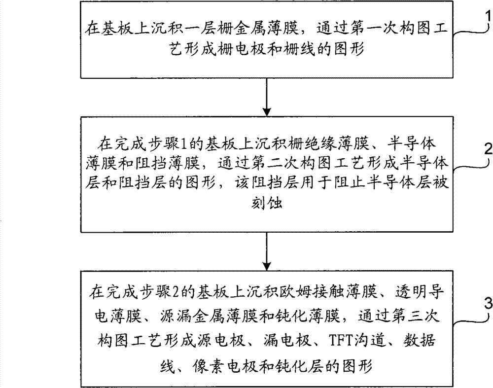
[0027] Such as figure 1 Shown is the flow chart of the TFT-LCD array substrate manufacturing method of the present invention, including:

[0028] Step 1, depositing a layer of gate metal thin film on the substrate, and forming the pattern of gate electrode and gate line through the first patterning process;

[0029] Step 2. Depositing a gate insulating film, a semiconductor film and a barrier film on the substrate completed in step 1, and forming a pattern of the semiconductor layer and the barrier layer through a second patterning process, the barrier layer is used to prevent the semiconductor layer from being etched;

[0030] Step 3. Deposit ohmic contact film, transparent conductive film, source-drain metal film and passivation film on the substrate after step 2, and form source electrode, drain electrode, channel, data line, pixel electrode and Graphics of the passivation layer.

[0031] The specific implementation process of each step is introduced in detail below.

[...


PUM

PropertyMeasurementUnit
thicknessaaaaaaaaaa
thicknessaaaaaaaaaa
thicknessaaaaaaaaaa

Abstract

The invention relates to a thin film transistor liquid crystal display (TFT-LCD) array substrate and a manufacturing method thereof, wherein the manufacturing method comprises the following steps of: 1, depositing a gate metal thin film on a substrate, forming a figure consisting of a gate electrode and a gate line through a first-time composition process; 2, depositing a gate insulating thin film, a semiconductor thin film and a barrier thin film on the substrate subjected to the step 1, forming figures of a semiconductor layer and a barrier layer through a second-time composition process, wherein the barrier layer is used for preventing the semiconductor layer from being etched; and 3, depositing an ohmic contact thin film, a transparent conductive thin film, a source-drain metal thin film and a passivated thin film on the substrate subjected to the step 2, and forming the figures of a source electrode, a drain electrode, a thin film transistor (TFT) channel, a data line, a pixel electrode and a passivation layer through a third-time composition process. The invention can reduce the thickness of the semiconductor layer and the off-state current of a TFT and enhance the performance of the TFT by adopting three times of the composition processes and arranging the barrier layer between the semiconductor layer and an ohmic contact layer in a clamping way.

Description

technical field [0001] The invention relates to a manufacturing method of a thin film transistor liquid crystal display, in particular to a thin film transistor liquid crystal display (Thin Film Transistor Liquid Crystal Display, TFT-LCD for short) array substrate and a manufacturing method thereof. Background technique [0002] TFT-LCD has the characteristics of small size, low power consumption, and no radiation, and occupies a dominant position in the current flat panel display market. For TFT-LCD, the array substrate structure and manufacturing process determine its product performance, yield and price. [0003] In order to effectively reduce the price of TFT-LCD and increase the yield, the manufacturing process of the TFT-LCD array substrate structure has been gradually simplified. Composition (4mask) process. [0004] In the prior art, a gray-tone or half-tone mask is used in the four-step patterning process, and the active layer, data lines, source electrodes, drain...

Claims


Application Information

Patent Timeline
Patent Type & Authority Patents(China)
IPC IPC(8): G02F1/1362H01L27/12H01L21/84
CPCH01L27/1288
Inventor 刘翔
Owner BOE TECH GRP CO LTD
Why Eureka
Try Eureka