Manufacture method of TFT substrate and manufactured TFT substrate

a manufacturing method and technology of tft elements, applied in the field of display technology, can solve the problems of asymmetry of tft structure and appearance of higher off state current, and achieve the effect of raising the electrical performance of tft elements

Active Publication Date: 2018-04-12
SHENZHEN CHINA STAR OPTOELECTRONICS TECH CO LTD
View PDF12 Cites 1 Cited by
  • Summary
  • Abstract
  • Description
  • Claims
  • Application Information

AI Technical Summary

Benefits of technology

[0006]An objective of the present invention is to provide a manufacture method of a TFT substrate, in which by designing the gate and the source or drain to be U shape structure to make both the path from the drain to the source and the path from the source to the drain in the TFT require passing through two offset structures and two overlapping structures, which does not only reduce the off state, raise the on state current but also makes the current path possess symmetry to avoid the influence of the asymmetry of the element structure to the current path in the LTPS TFT and to raise the electrical performance of the TFT element.

Problems solved by technology

However, the defect due to the grain existence in the LTPS will lead to the appearance of the higher off state current as the LTPS TFT is in off state.
However, in one LTPS TFT, as the source and drain respectively utilize the offset structure and the overlap structure, it leads to the asymmetry of the TFT structure.

Method used


Image

  • Manufacture method of TFT substrate and manufactured TFT substrate
  • Manufacture method of TFT substrate and manufactured TFT substrate
  • Manufacture method of TFT substrate and manufactured TFT substrate

Examples


Embodiment Construction

[0052]For better explaining the technical solution and the effect of the present invention, the present invention will be further described in detail with the accompanying drawings and the specific embodiments.

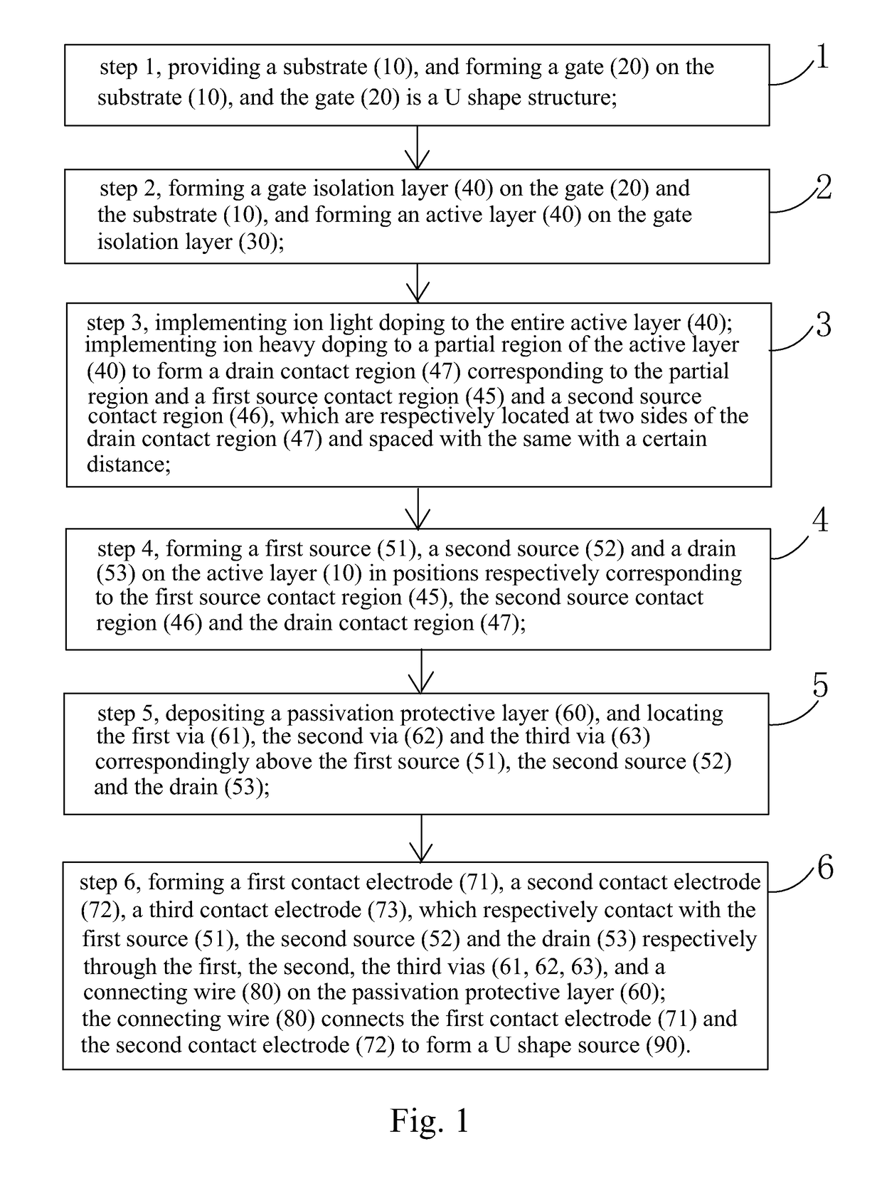
[0053]Please refer to FIG. 1. The present invention provides a manufacture method of a TFT substrate, comprising steps of:

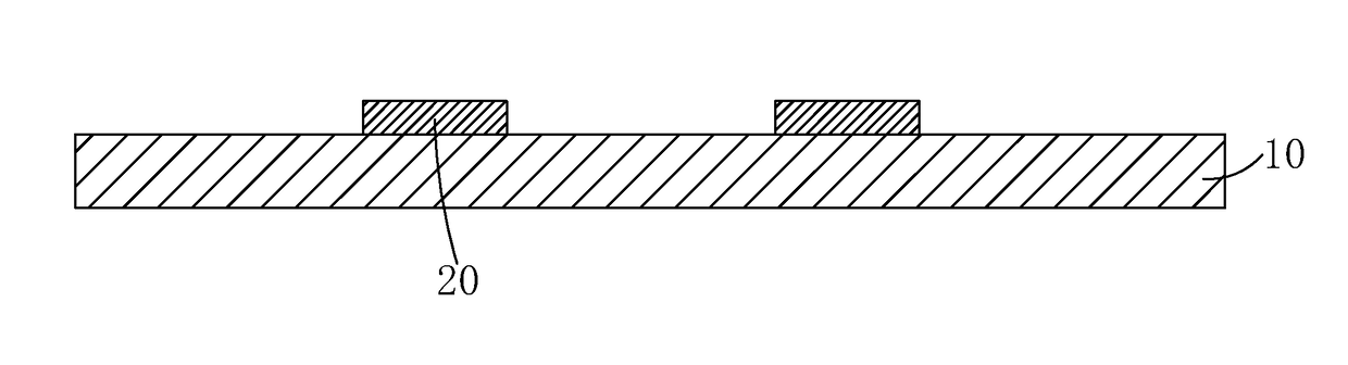
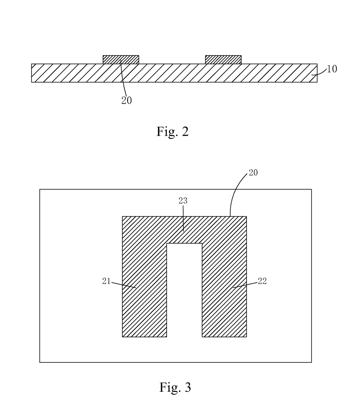
[0054]step 1, as shown in FIGS. 2-3, providing a substrate 10, and forming a gate 20 on the substrate 10, and the gate 20 is a U shape structure, comprising a first vertical part 21, a second vertical part 22 and a transverse connecting part 23, connecting corresponding end parts of the first vertical part 21 and the second vertical part 22.

[0055]Specifically, the manufacture method of the gate 20 can be: depositing a metal layer on the substrate 10, and employing one mask for patterning the metal layer to obtain the gate 20.

[0056]Specifically, material of the metal layer is metal material, such as aluminum (Al), molybdenum (Mo), copper (Cu) and silver (Ag)...


PUM


Abstract

The present invention provides a manufacture method of a TFT substrate and a manufactured TFT substrate. By locating the first channel region and the first lightly doped offset region between the first source and the drain, and locating the second channel region and the second lightly doped offset region between the second source and the drain, and forming the first overlapping region and the second overlapping region respectively between the drain and the gate and between the second source and the gate, thus, the paths of the current flowing from the first, the second sources to the drain and the current flowing from the drain to the first, the second sources are the same. Namely, the current path from source to the drain and the current path from the drain to the source are the same. According, the symmetry of the TFT structure is realized.

Description

FIELD OF THE INVENTION[0001]The present invention relates to a display technology field, and more particularly to a manufacture method of a TFT substrate and a manufactured TFT substrate.BACKGROUND OF THE INVENTION[0002]The OLED is a flat panel display technology which has great prospects for development. It possesses extremely excellent display performance, and particularly the properties of self-illumination, simple structure, ultra thin, fast response speed, wide view angle, low power consumption and capability of realizing flexible display, and therefore is considered as the “dream display”. Meanwhile, the investment for the production equipments is far smaller than the TFT-LCD. It has been favored by respective big display makers and has become the main selection of the third generation display element of the display technology field. At present, the OLED has reached the point before mass production. With the further research and development, the new technologies constantly app...

Claims


Application Information

Patent Timeline
Patent Type & Authority Applications(United States)
IPC IPC(8): H01L29/66H01L29/786H01L21/02H01L21/77
CPCH01L29/6675H01L29/786H01L21/02667H01L21/77H01L27/1214H01L27/1259H01L29/66765H01L29/78624H01L29/78645H01L29/78678
Inventor CHI, SHIPENG
Owner SHENZHEN CHINA STAR OPTOELECTRONICS TECH CO LTD
Why Eureka
Try Eureka