Thin film transistor and display array substrate using same

A technology of thin film transistor and organic barrier layer, applied in transistors, electro-solid devices, semiconductor devices, etc., can solve the problems of frequency characteristics, inability to meet panel requirements, etc., and achieve the effect of improving TFT performance

Inactive Publication Date: 2015-03-18
HONG FU JIN PRECISION IND (SHENZHEN) CO LTD +1
View PDF3 Cites 2 Cited by
  • Summary
  • Abstract
  • Description
  • Claims
  • Application Information

AI Technical Summary

Problems solved by technology

However, since the etching barrier layer must meet a certain thickness requirement, such as greater than 1 micron, the channel width between the source and the drain is usually maintained at about 10 microns due to the influence of the thickness when the contact hole is formed by exposure to yellow light, which cannot be achieved. If it is reduced to a smaller range, it will not only affect the characteristics of the thin film transistor itself, such as frequency characteristics, but also cannot meet the requirements of high resolution (High Resolution HD) panels.

Method used


Image

  • Thin film transistor and display array substrate using same
  • Thin film transistor and display array substrate using same
  • Thin film transistor and display array substrate using same

Examples


Embodiment Construction

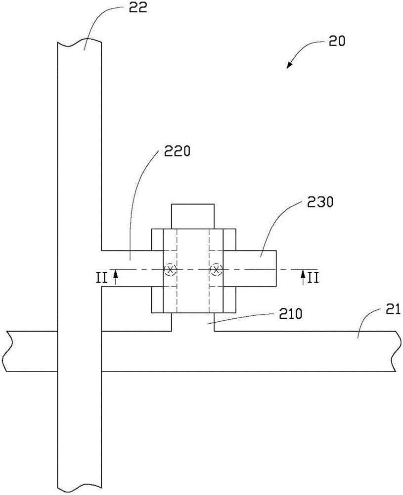
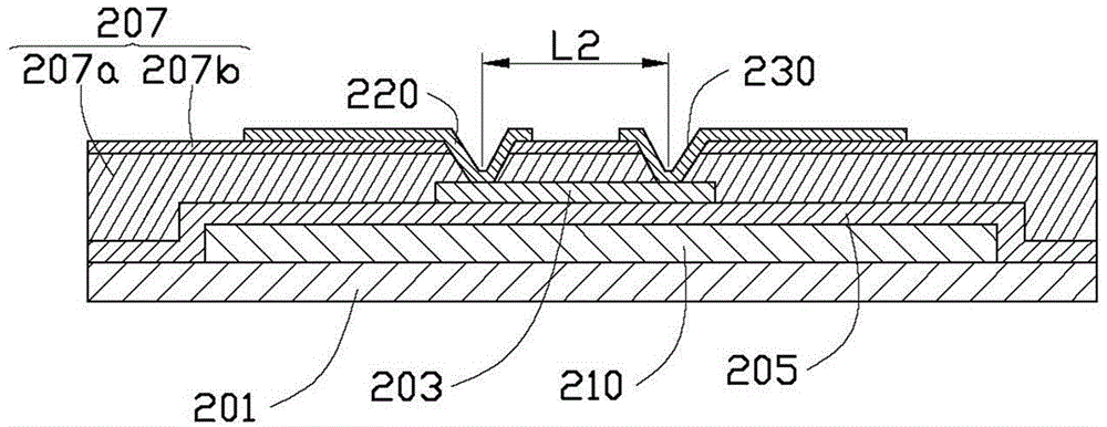
[0021] see figure 1 , figure 1 It is a schematic plan view of a part of a pixel area of ​​a display array substrate according to an embodiment of the present invention. The display array substrate 20 includes a plurality of gate lines 21 parallel to each other, and a plurality of data lines 22 parallel to each other and insulated from and crossing the gate lines. A thin-film transistor (thin-film transistor, TFT) 200 is arranged at the intersection of each gate line 11 and a data line 12, and the thin-film transistor 200 includes a gate 210 connected to the gate line 21 for an external gate driver (not shown) shown), the source 220 connected to the data line 22 is used to receive the data signal output from an external data driver (not shown), and the drain 230 is spaced apart from the source 220 .

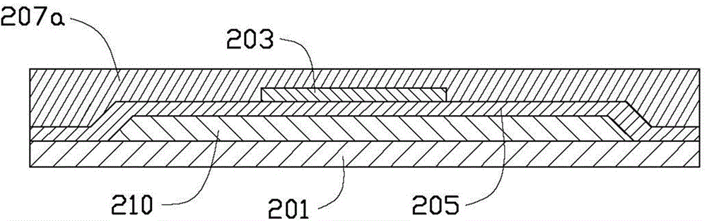
[0022] When the gate signal voltage output by the gate line 210 is higher than the threshold voltage of the thin film transistor 200, the channel layer 203 formed inside the thi...


PUM


Abstract

The invention provides a thin film transistor. The thin film transistor includes the following components of: a gate; an gate insulating layer covering the gate; a channel layer which is arranged on the gate insulating layer and is corresponding to the gate; an etching barrier layer which covers the channel layer and at least comprises one organic barrier layer and a hard mask layer arranged on the organic barrier layer in a layer-upon-layer manner, wherein the organic barrier layer is a cured transparent organic material layer, and the hard mask layer is formed on the surface of the organic barrier layer and is used for enhancing the hardness of the organic barrier layer, wherein the surface of the organic barrier layer faces a direction opposite to the channel layer; two contact holes which pass through the etching barrier layer; as well as a source and a drain which are connected with the channel layer through the two contact holes. The invention also provides a display array substrate using the thin film transistor.

Description

technical field [0001] The invention relates to a thin film transistor and a display array substrate using the thin film transistor. Background technique [0002] A thin film transistor (Thin Film Transistor, TFT) that uses a metal oxide semiconductor (Metal Oxide Semiconductor) to form a channel has been gradually and widely used in the display field as a switch component. In the thin film transistor manufacturing process, because the metal oxide semiconductor is sensitive to the back-end process, such as the wet etching (Wet-Etching) process used to form the source and drain of the thin film transistor, it will form an etch on the metal oxide semiconductor layer. The blocking layer protects the properties of the metal oxide semiconductor layer. However, since the etching barrier layer must meet a certain thickness requirement, such as greater than 1 micron, the channel width between the source and the drain is usually maintained at about 10 microns due to the influence of...

Claims


Application Information

Patent Timeline
Patent Type & Authority Applications(China)
IPC IPC(8): H01L29/786H01L29/10H01L27/12
CPCH01L29/7869H01L21/4757H01L27/1214H01L29/66969H01L29/78696
Inventor 吴逸蔚陆一民张炜炽林辉巨高逸群方国龙
Owner HONG FU JIN PRECISION IND (SHENZHEN) CO LTD
Why Eureka
Try Eureka