Method for electrical coupling and electric coupling arrangement

a technology of electrical coupling and electrical coupling, which is applied in the direction of electrical apparatus, semiconductor/solid-state device details, semiconductor devices, etc., can solve problems such as stress on substrates and/or semiconductor chips

Active Publication Date: 2016-12-01
IBM CORP +3
View PDF4 Cites 38 Cited by
  • Summary
  • Abstract
  • Description
  • Claims
  • Application Information

AI Technical Summary

Problems solved by technology

This process can cause stress to the substrate and / or the semiconductor chip due to differing thermal expansion coefficients.

Method used


Image

  • Method for electrical coupling and electric coupling arrangement
  • Method for electrical coupling and electric coupling arrangement
  • Method for electrical coupling and electric coupling arrangement

Examples


Embodiment Construction

[0017]In this disclosure, embodiments for methods for electrically coupling at least two elements are disclosed. For example, the methods disclosed herein may include coupling a conductive pad on a substrate (first element) with a pillar protruding from a die of a microelectronic chip (second element). Often, a plurality of pads and corresponding pillars are arranged in arrays that are coupled to each other.

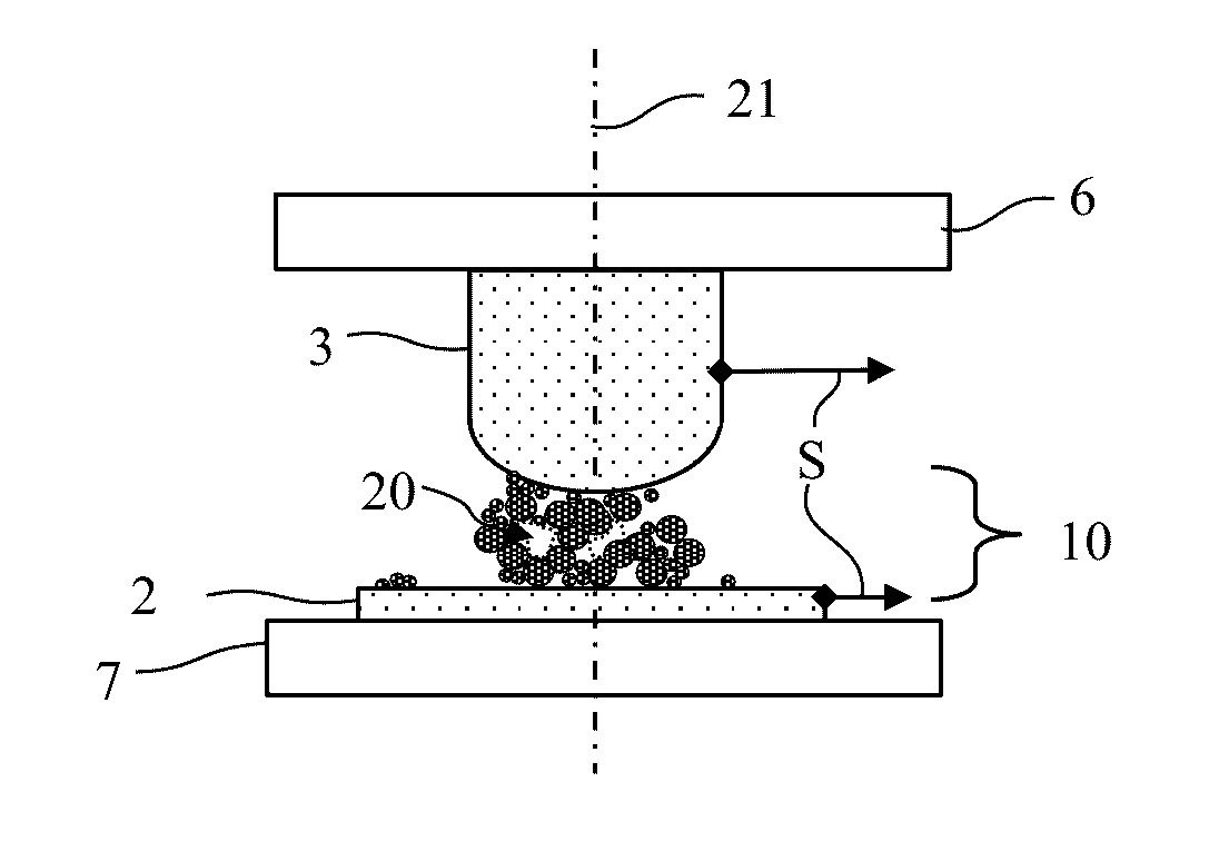
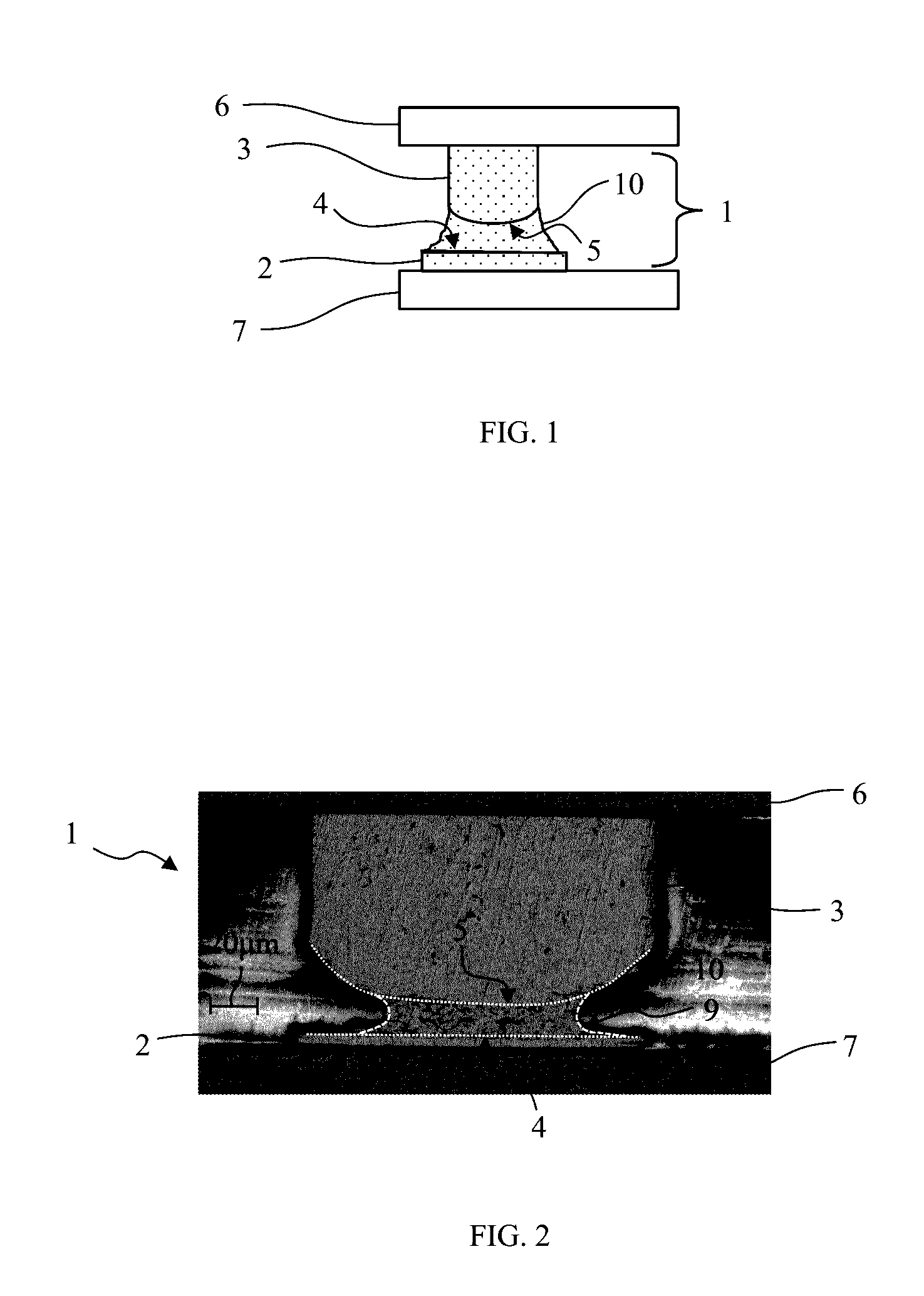
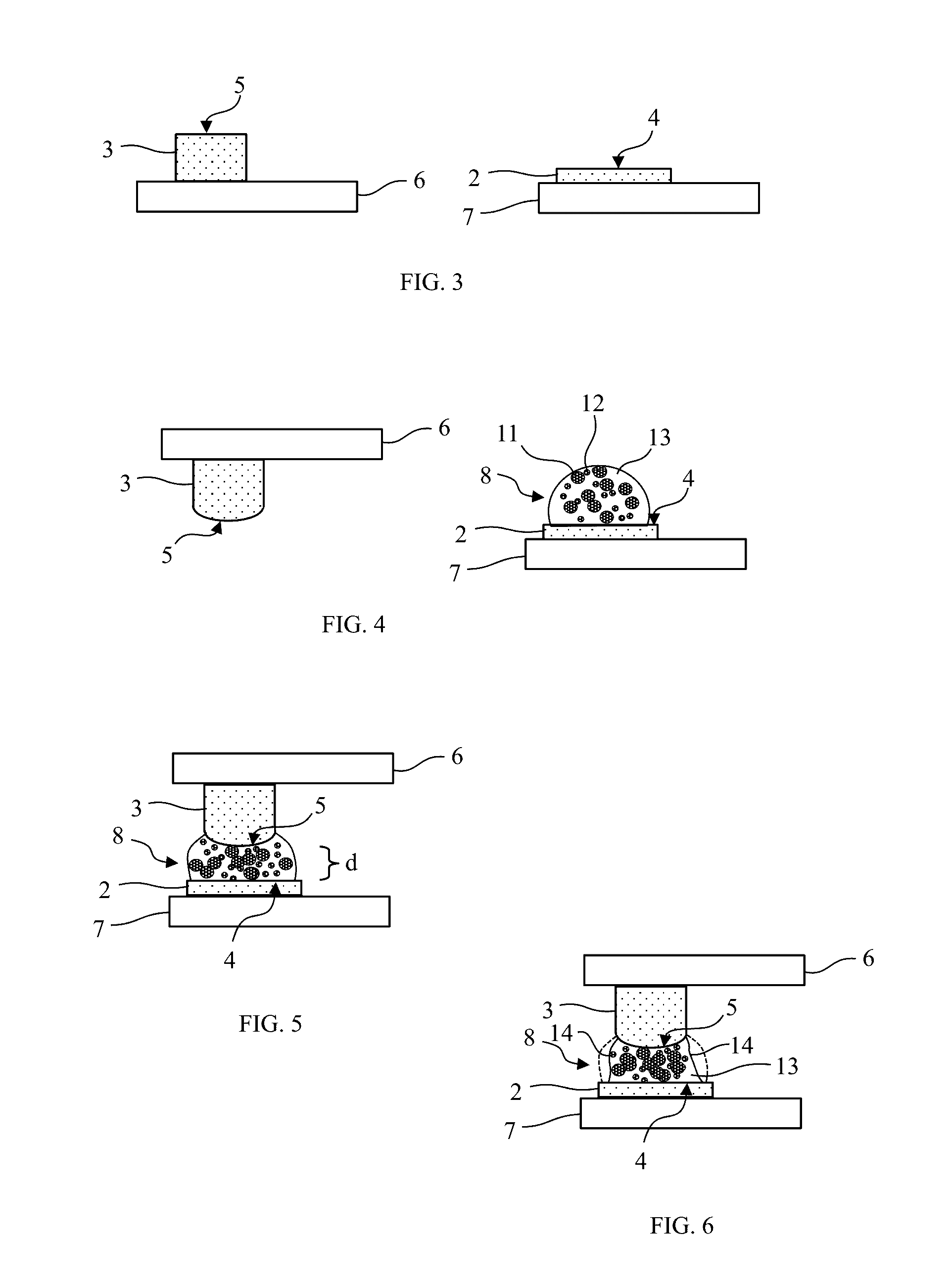
[0018]FIG. 1 shows a schematic cross-sectional view of an embodiment of a coupling arrangement 1 between a chip 6 and a substrate 7. In FIG. 1, an electrically conducting pillar 3 is shown protruding from the chip 6. The pillar 3 has a cylindrical shape and has a front surface 5 facing towards a pad 2. The front surface forms a copula-like surface of the pillar 3. Opposite to the front surface 5 of the pillar 3 is an electrically conducting pad 2 arranged on the substrate 7. The pad 2 has an essentially flat surface 4. In the gap between the front surface 5 of the pillar 3 and th...


PUM


Abstract

A method for electrically coupling a pad and a front face of a pillar, including shaping the front face pillar, the front face having at least partially a convex surface, applying a suspension to the front face or to the pad, wherein the suspension includes a carrier fluid, electrically conducting microparticles and electrically conducting nanoparticles, arranging the front face of the pillar opposite to the pad at a distance such that the carrier fluid bridges at least partially a gap between the front face of the pillar and the pad, evaporating the carrier fluid thereby confining the microparticles and the nanoparticles, and thereby arranging the nanoparticles and the microparticles as percolation paths between the front face of the pillar and the pad, and sintering the arranged nanoparticles for forming metallic bonds at least between the nanoparticles and / or between the nanoparticles and the front face of the pillar or the pad.

Description

BACKGROUND[0001]Technical Field[0002]The invention relates to a method for electrically coupling at least two elements and to a coupling arrangement for electrically coupling to elements.[0003]Related Art[0004]In electronic devices, electric coupling is conventionally implemented, for example, by soldering electric terminals to pads or printed circuitry using a solder material. For example, microelectronic devices are often implemented as semiconductor chips sometimes having bond pads that are placed in regular arrays on the die.[0005]A currently used scheme for conductively coupling bond pads with corresponding contact pads on the substrate is a flip-chip interconnection. A flip-chip package requires bonds of solder that are soldered and form the electrical connection between the chip and the substrate. During the soldering process, the solder needs to be heated above its melting temperature. This process can cause stress to the substrate and / or the semiconductor chip due to differ...

Claims


Application Information

Patent Timeline
Patent Type & Authority Applications(United States)
IPC IPC(8): H01L23/00
CPCH01L24/81H01L2224/29647H01L24/27H01L24/29H01L24/13H01L24/73H01L24/08H01L24/03H01L2224/8384H01L2224/16227H01L2224/1607H01L2224/2957H01L2224/08238H01L2224/05647H01L2224/13147H01L24/11H01L2224/13005H01L2224/11822H01L2224/13499H01L2224/13019H01L2224/13294H01L2224/13347H01L2224/16058H01L2224/16238H01L2224/81191H01L2224/81193H01L2224/81447H01L2224/8184H01L2924/351H01L2924/00014H01L2924/20751H01L2924/20752H01L2924/20753H01L2924/20754
Inventor BRUNSCHWILER, THOMAS J.DIXON, RICHARDVISSER TAKLO, MAAIKE M.WUNDERLE, BERNHARDYU, KERRYZUERCHER, JONAS
Owner IBM CORP
Why Eureka
Try Eureka