Imaging device, and controlling method of imaging device

a technology of imaging device and control method, which is applied in the field of imaging subject technology, can solve problems such as the deterioration of light-emitting elements, and achieve the effect of improving the quality of light-emitting elements

Active Publication Date: 2016-12-01
SEIKO EPSON CORP
View PDF4 Cites 3 Cited by
  • Summary
  • Abstract
  • Description
  • Claims
  • Application Information

AI Technical Summary

Benefits of technology

[0017]In the controlling method according to the aspect of the invention, the imaging portion may include a plurality of light-receiving elements which overlap the transmission region in a plan view, and in the first period in which the plurality of first light-emitting elements are turned on, light received by the light-receiving elements respectively corresponding to the plurality of second light-emitting elements may be regarded as valid and light received by the light-receiving elements respectively corresponding to the plurality of first light-emitting elements may be regarded as not valid, and in the first period in which the plurality of second light-emitting elements are turned on, light received by the light-receiving elements respectively corresponding to the plurality of first light-emitting elements may be regarded as valid and light received by the light-receiving elements respectively corresponding to the plurality of second light-emitting elements may be regarded as not valid. In this method, in the first period in which the plurality of first light-emitting elements are turned on, light received by the light-receiving elements that overlap the transmission region corresponding to the first light-emitting elements is regarded as not valid, and the light-receiving elements that overlap the transmission region corresponding to the second light-emitting elements are regarded as valid. In addition, in the first period in which the plurality of second light-emitting elements are turned on, light received by the light-receiving elements that overlap the transmission region corresponding to the second light-emitting elements is regarded as not valid, and the light-receiving elements that overlap the transmission region corresponding to the first light-emitting elements are regarded as valid. Therefore, there is an advantage that the effect (for example, saturation of the charge quantity that occurs in the light-receiving elements) of the light emitted from the first light-emitting elements (the second light-emitting elements) toward the imaging portion side can be suppressed. In addition, “being not valid” for the light received by the light-receiving element means that the light received by the corresponding light-receiving element is not reflected in the result of the imaging. For example, not outputting a detection signal from the corresponding light-receiving element or discarding or ignoring the detection signal output from the corresponding light-receiving element is implicit in the meaning of “being not valid” for the light received by the light-receiving element.

Problems solved by technology

However, since the light-emitting element emits light in both of the first and second stages, there is a problem in that the deterioration of the light-emitting element proceeds.
In addition, “being not valid” for the light received by the light-receiving element means that the light received by the corresponding light-receiving element is not reflected in the result of the imaging.

Method used


Image

  • Imaging device, and controlling method of imaging device
  • Imaging device, and controlling method of imaging device
  • Imaging device, and controlling method of imaging device

Examples


embodiment

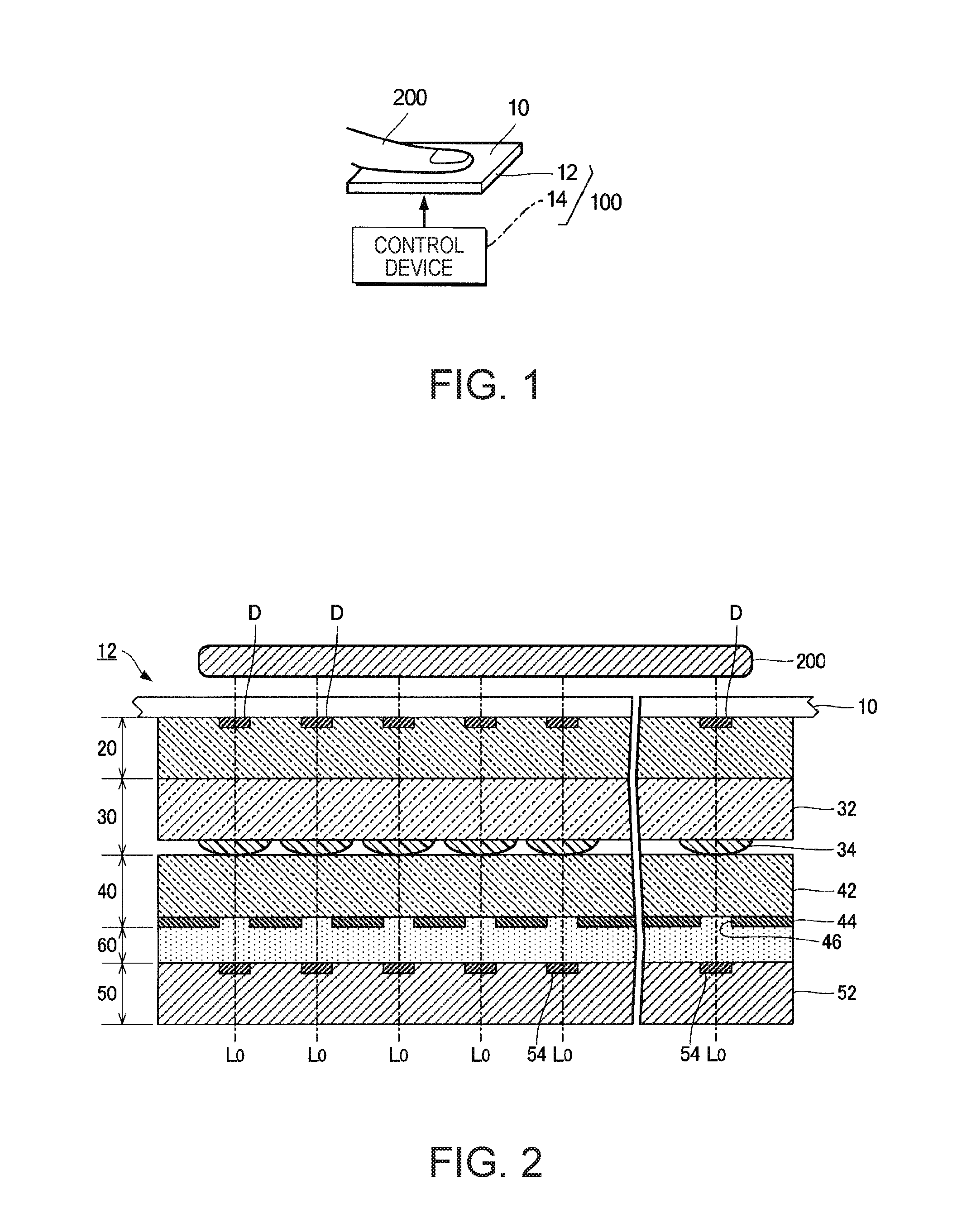
[0031]FIG. 1 is a schematic view of a biological information generation device 100 to which an imaging device 12 according to a preferred embodiment of the invention is applied. The biological information generation device 100 is a measurement device that images a subject 200 such as a finger of an object to be tested and measures biological information (for example, an oxygen saturation degree or blood sugar level) according to the result of the imaging, and includes the imaging device 12 and a control device 14. The imaging device 12 is a device that images the subject 200, and the control device 14 controls operations of the imaging device 12 and generates biological information. For example, the control device 14 is implemented as a central processing unit (CPU) that executes operations of controlling the imaging device 12 and generating biological information by executing programs stored in a storage device (not illustrated).

[0032]FIG. 2 is a sectional view of the imaging devic...

modification example

[0076]The above-described embodiment can be modified in various manners. Specific modification examples are described below. Two or more examples arbitrarily selected from the following description may be appropriately combined in a range in which there is no contradiction therebetween.

[0077](1) The configuration of the unit circuit K is not limited to the illustration of FIG. 6. For example, as illustrated in FIG. 9, it is possible to provide a transistor TRS between the first electrode E1 of the light-emitting element DP and a wire 97 to which a voltage VSS is supplied. The voltage VSS is a voltage lower than the voltage VL (for example, ground voltage). The gate of the transistor TRS is connected to the gate of the transistor TDR. In a case where the drive signal S[n] is set to the voltage VL when the scanning line 95 in the m-th row is selected, the transistor TRS is maintained in the OFF state. Therefore, the light-emitting element DP is turned on as in the above-described embo...


PUM


Abstract

An imaging device includes: an illumination portion which includes a light-transmitting transmission region and a light-shielding non-transmission region, has a plurality of simultaneous light-emitting elements that have a light-transmitting property, include a plurality of first light-emitting elements in which turning-on and turning-off are simultaneously controlled and a plurality of second light-emitting elements in which turning-on and turning-off are simultaneously controlled, and are provided in the transmission region, and has a plurality of individual light-emitting elements in which turning-on and turning-off are individually controlled and which are provided in the non-transmission region; an imaging portion which receives light that is reflected from a subject illuminated by the illumination portion and is transmitted through the transmission region; and a switching portion which selectively turns on the plurality of first light-emitting elements and the plurality of second light-emitting elements in a first period in which the plurality of individual light-emitting elements are turned off, and turns off the plurality of simultaneous light-emitting elements in a second period in which the plurality of individual light-emitting elements are turned on.

Description

BACKGROUND[0001]1. Technical Field[0002]The present invention relates to a technique for imaging a subject.[0003]2. Related Art[0004]Various types of imaging devices for imaging a subject have been proposed. For example, JP-A-2014-67577 discloses a configuration in which a light-receiving element receives light reflected from a subject when the subject is illuminated by a light-emitting element containing an organic EL material, thereby imaging the subject.[0005]However, for example, in a case where a vein pattern of a finger is imaged, a sequential order, in which the entirety of the finger is illuminated and imaged in a first stage and a portion corresponding to a vein pattern specified from the result of the imaging is partially illuminated and imaged in a second stage, is postulated. However, since the light-emitting element emits light in both of the first and second stages, there is a problem in that the deterioration of the light-emitting element proceeds.SUMMARY[0006]An adva...

Claims


Application Information

Patent Timeline
Patent Type & Authority Applications(United States)
IPC IPC(8): H04N5/225
CPCH04N5/2256H04N23/56H04N23/55H10K59/65G06V40/1318
Inventor TOYA, TAKASHIMIYASAKA, MITSUTOSHI
Owner SEIKO EPSON CORP
Why Eureka
Try Eureka