Method And System For Large Silicon Photonic Interposers By Stitching

a technology of photonic interposers and silicon, applied in the field of semiconductor processing, can solve the problems of cable bulk penalties, large power requirements, and complex structure, and achieve the effects of small improvement in reach, limited scalability, and limited scalability

Active Publication Date: 2016-12-08
CISCO TECH INC
View PDF6 Cites 19 Cited by
  • Summary
  • Abstract
  • Description
  • Claims
  • Application Information

AI Technical Summary

Benefits of technology

[0007]A system and/or method for large silicon photonic interposers by stitching, substantially as shown in

Problems solved by technology

They can be mitigated to some extent with equalization, coding, and shielding, but these techniques require considerable

Method used


Image

  • Method And System For Large Silicon Photonic Interposers By Stitching
  • Method And System For Large Silicon Photonic Interposers By Stitching
  • Method And System For Large Silicon Photonic Interposers By Stitching

Examples


Embodiment Construction

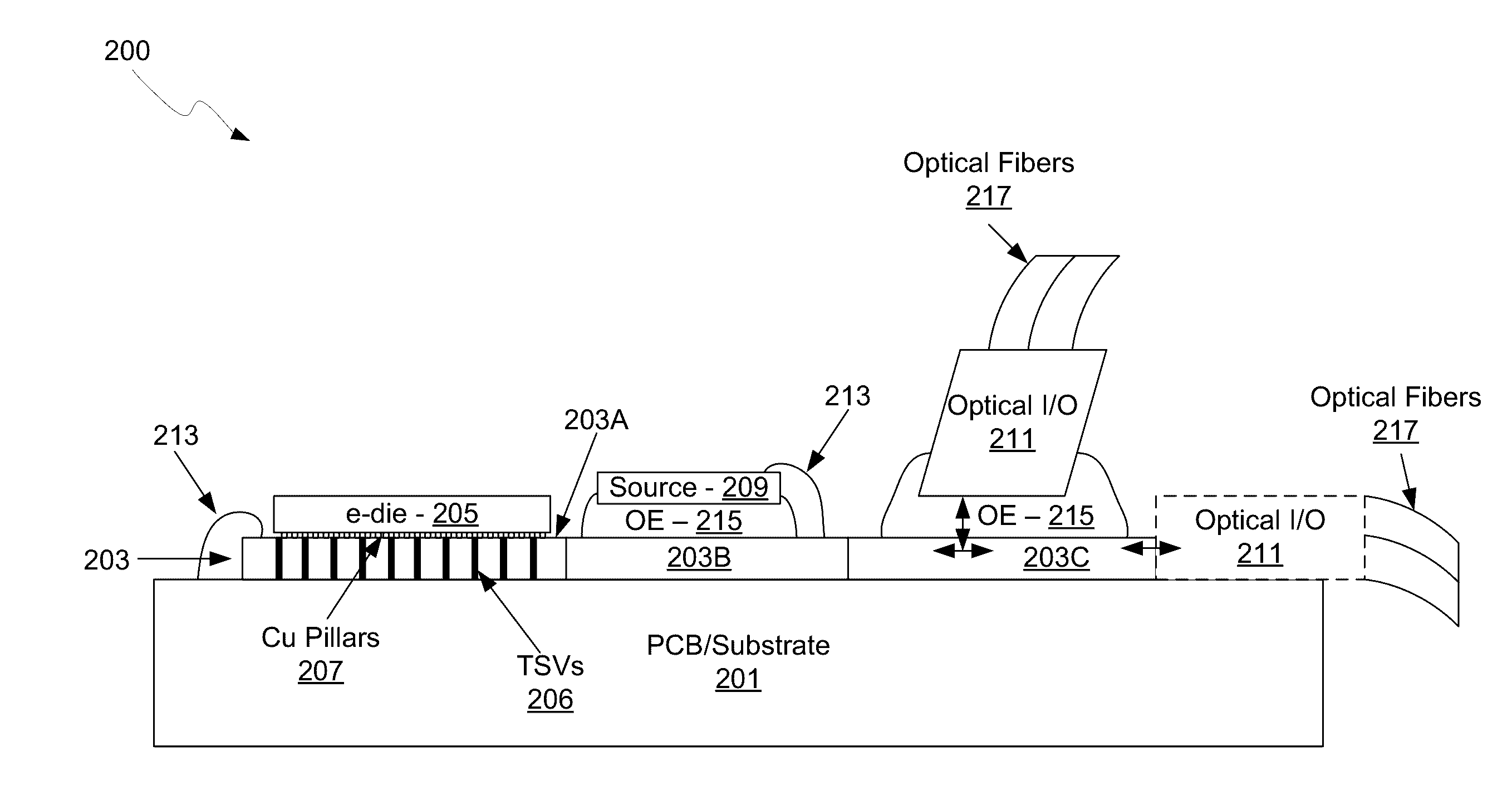
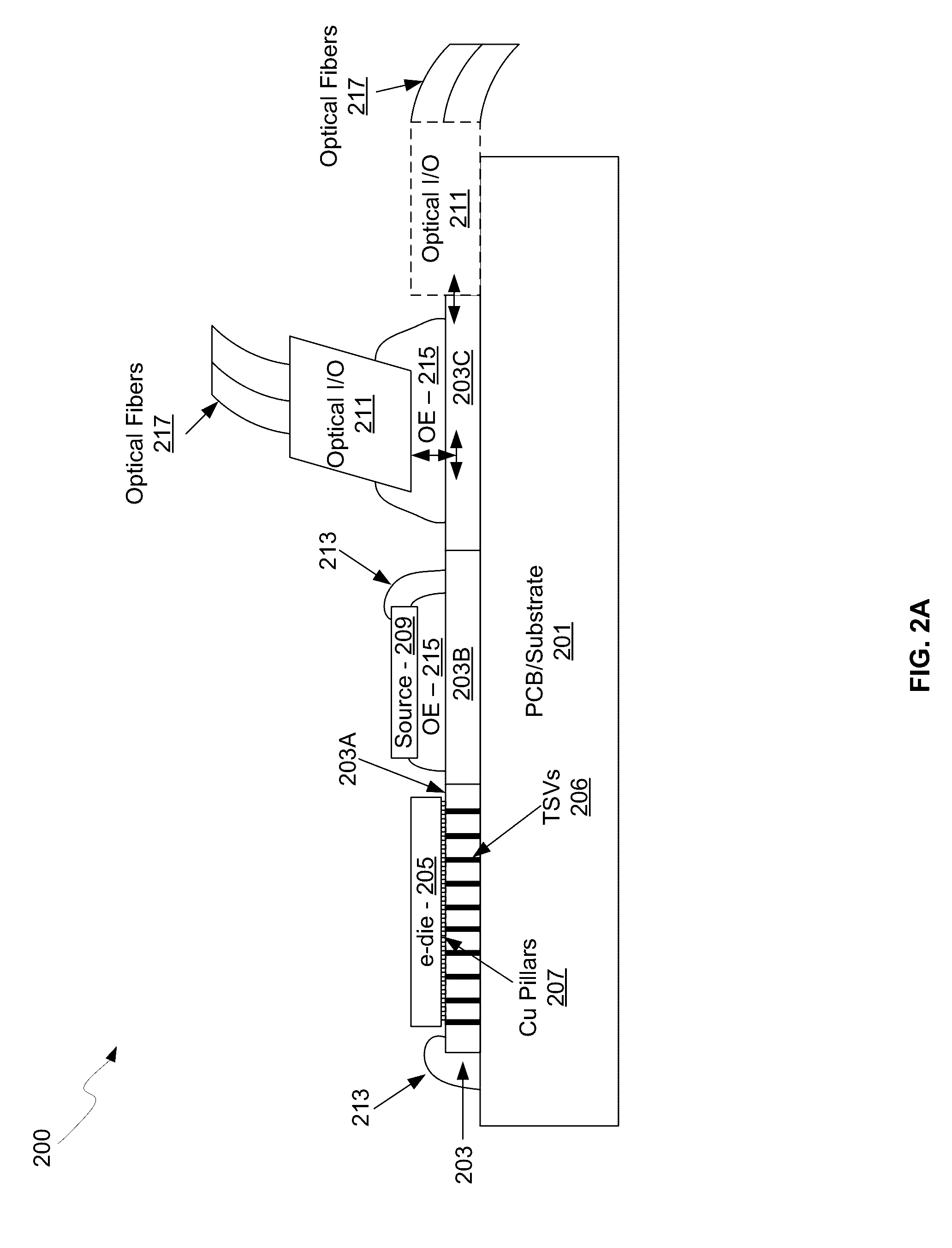
[0017]Certain aspects of the disclosure may be found in a method and system for large silicon photonic interposers by stitching. Example aspects of the disclosure may comprise an integrated optical communication system comprising one or more complementary metal-oxide semiconductor (CMOS) electronics die coupled to a silicon photonic interposer, where the silicon photonic interposer comprises a plurality of reticle sections and where the integrated optical communication system is operable to communicate an optical signal between two of the plurality of reticle sections utilizing a waveguide. The waveguide may comprise a taper region at a boundary between the two reticle sections, the taper region expanding an optical mode of the communicated optical signal prior to the boundary and narrowing the optical mode after the boundary. A continuous wave (CW) optical signal may be received in a first of the plurality of reticle sections in the silicon photonic interposer from an optical sourc...


PUM


Abstract

Methods and systems for large silicon photonic interposers by stitching are disclosed and may include, in an integrated optical communication system including CMOS electronics die coupled to a silicon photonic interposer, where the interposer includes a plurality of reticle sections: communicating an optical signal between two of the plurality of reticle sections utilizing a waveguide. The waveguide may include a taper region at a boundary between the two reticle sections, the taper region expanding an optical mode of the communicated optical signal prior to the boundary and narrowing the optical mode after the boundary. A continuous wave (CW) optical signal may be received in a first of the reticle sections from an optical source external to the interposer. The CW optical signal may be received in the interposer from an optical source assembly coupled to a grating coupler in the first of the reticle sections in the silicon photonic interposer.

Description

CROSS-REFERENCE TO RELATED APPLICATIONS / INCORPORATION BY REFERENCE[0001]This application makes reference to and claims priority to U.S. Provisional Application Ser. No. 62 / 230,290 filed on Jun. 2, 2015. This application also makes reference to U.S. Application Ser. No. 13 / 422,776, filed on Mar. 16, 2012. Each of the above stated applications is hereby incorporated herein by reference in its entirety.FEDERALLY SPONSORED RESEARCH OR DEVELOPMENT[0002][Not Applicable][MICROFICHE / COPYRIGHT REFERENCE[0003][Not Applicable]FIELD[0004]Certain embodiments of the disclosure relate to semiconductor processing. More specifically, certain embodiments of the disclosure relate to a method and system for large silicon photonic interposers by stitching.BACKGROUND[0005]As data networks scale to meet ever-increasing bandwidth requirements, the shortcomings of copper data channels are becoming apparent. Signal attenuation and crosstalk due to radiated electromagnetic energy are the main impediments enco...

Claims


Application Information

Patent Timeline
IPC IPC(8): H04B10/80G02B6/34G02B6/42G02B6/122
CPCH04B10/801G02B6/4279G02B6/34G02B6/1228G02B6/428G02B6/4292G02B6/43H01R13/6461H01R13/6594H01R24/60H01R25/006H01R2107/00G02B6/12G02B6/1225G02B6/268G02B6/305G02B2006/12061H01R13/6471H01R13/6585H01R13/6586H01R13/6588
Inventor DE DOBBELAERE, PETERMEKIS, ATTILAMASINI, GIANLORENZO
Owner CISCO TECH INC
Why Eureka
Try Eureka