Active-matrix substrate, display panel and display device including the same

a technology of active matrix and substrate, which is applied in the direction of pulse technique, process and machine control, instruments, etc., can solve the problems of increasing the load on the gate line, and difficulty in driving the gate line at high speed, so as to reduce the dullness of the potential and achieve high speed

Active Publication Date: 2016-12-22
SHARP KK
View PDF0 Cites 19 Cited by
  • Summary
  • Abstract
  • Description
  • Claims
  • Application Information

AI Technical Summary

Benefits of technology

[0003]When a potential corresponding to a selection or non-selection state of a gate line is supplied to a gate line through one side of the active-matrix substrate that is parallel to the source lines, the potential becomes dull as it goes toward the distal end of the gate line. This requires a design that takes into consideration the position where a potential on a gate line becomes dull. JP 2004-538511 A, mentioned above, provides the gate driver and source driver along one side of the active-matrix substrate to make it possible to reduce the width of the portions of the picture frame region along the other three sides. However, according to JP 2004-538511 A, the distance of routing of the gate lines is greater than in conventional devices, increasing the load on the gate lines. As a result, a potential provided to a gate line becomes dull, making it difficult to drive the gate lines at high speed.
[0004]An object of the present invention is to provide a technique to reduce dullness of a potential provided to a line such as a gate line on the active-matrix substrate to enable driving the line at high speed and, at the same time, reduce the width of the picture frame region.
[0033]The arrangements of the present invention reduce dullness of a potential provided to a line on the active-matrix substrate to enable driving the lines at high speed.

Problems solved by technology

However, according to JP 2004-538511 A, the distance of routing of the gate lines is greater than in conventional devices, increasing the load on the gate lines.
As a result, a potential provided to a gate line becomes dull, making it difficult to drive the gate lines at high speed.

Method used


Image

  • Active-matrix substrate, display panel and display device including the same
  • Active-matrix substrate, display panel and display device including the same
  • Active-matrix substrate, display panel and display device including the same

Examples


first embodiment

Construction of Liquid Crystal Display Device

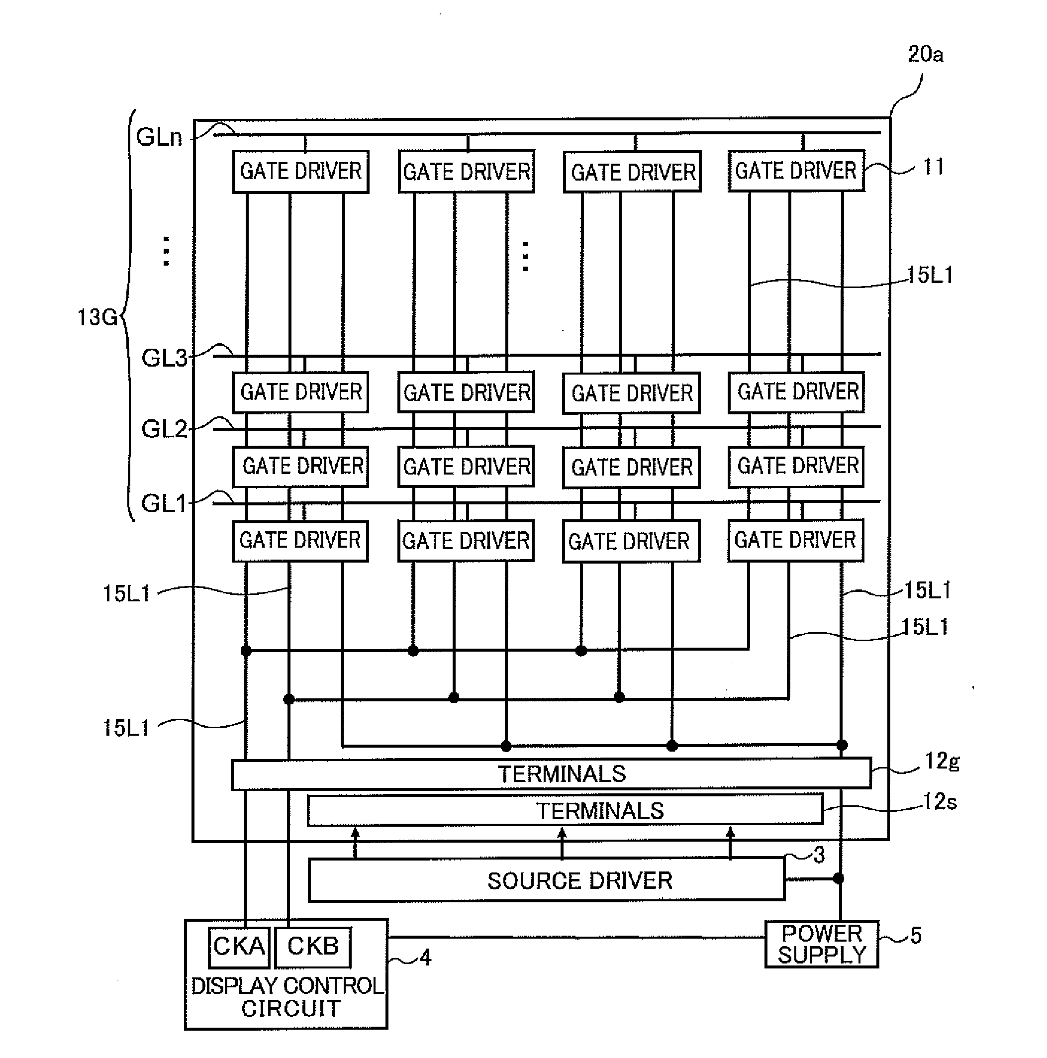
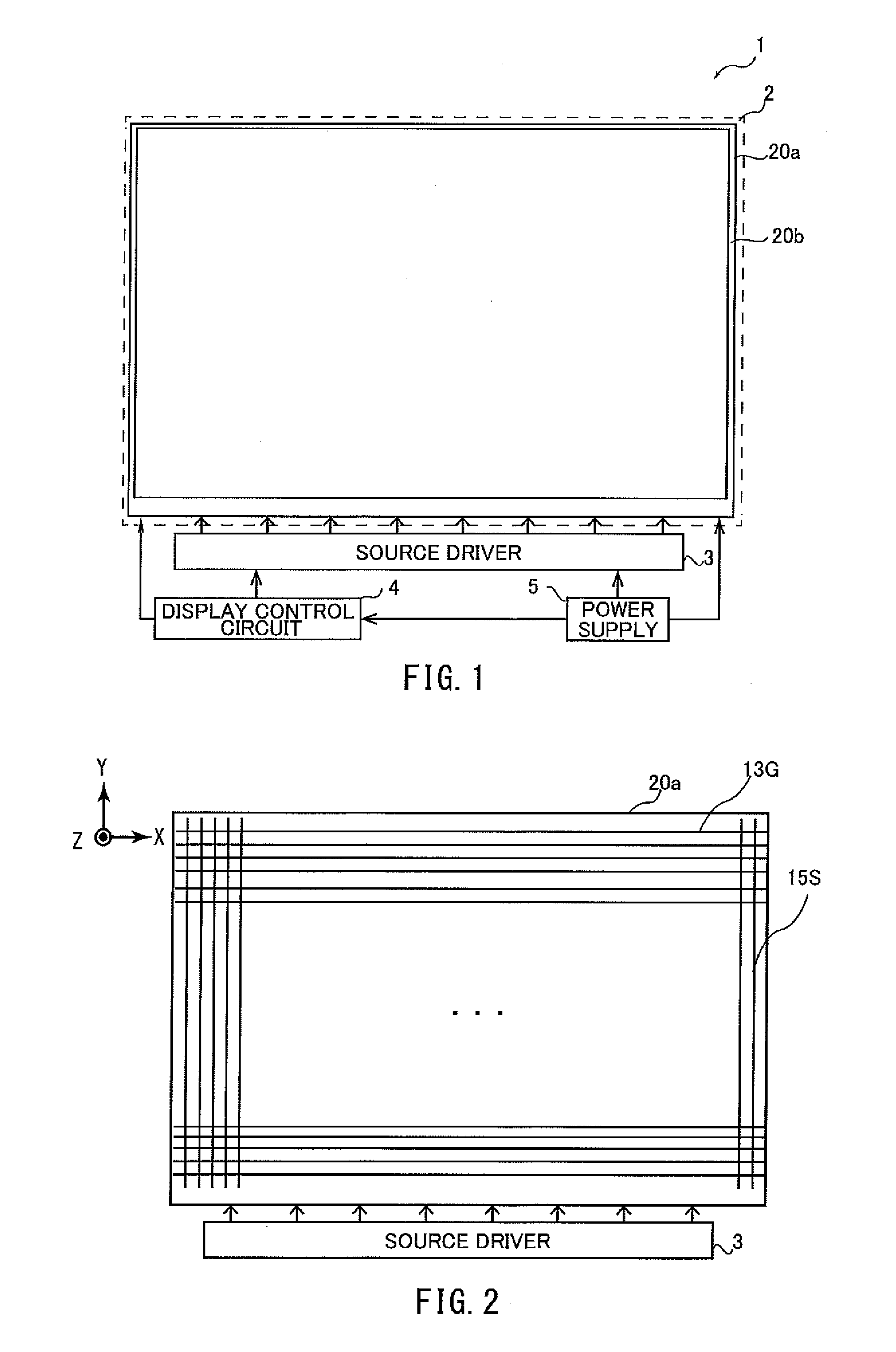
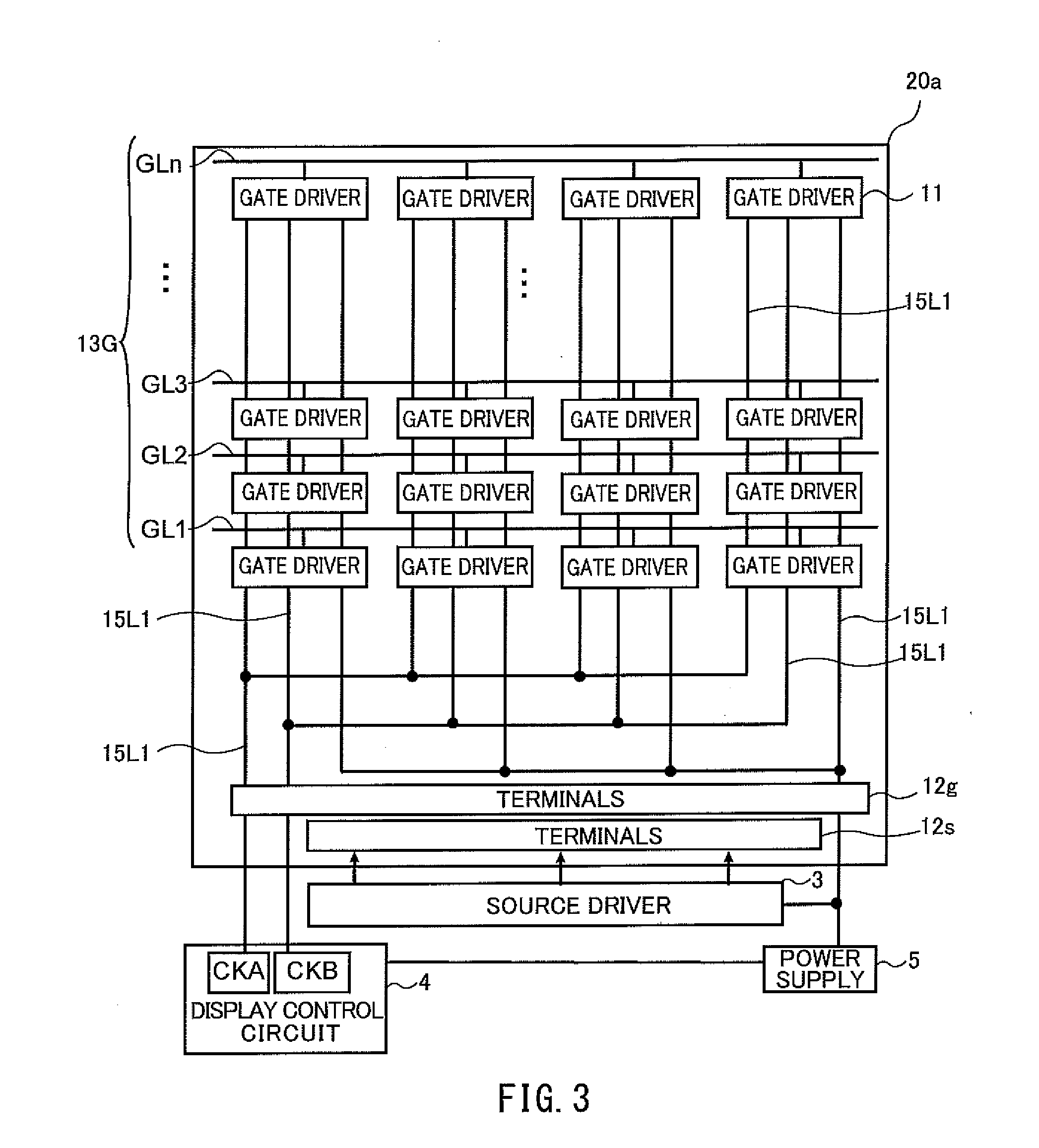
[0207]FIG. 1 is a schematic plan view of a liquid crystal display device according to the present embodiment. The liquid crystal display device 1 includes a display panel 2, a source device 3, a display control circuit 4, and a power supply 5. The display panel 2 includes an active-matrix substrate 20a, a counter-substrate 20b, and a liquid crystal layer (not shown) sandwiched between these substrates. Although not shown in FIG. 1, a polarizer is provided on the lower side of the active-matrix substrate 20a and another polarizer is provided on the upper side of the counter-substrate 20b. On the counter-substrate 20b are provided: a black matrix, red (R), green (G) and blue (B) color filters, and a common electrode (all not shown).

[0208]As shown in FIG. 1, the active-matrix substrate 20a is electrically connected with the source driver 3, which is provided on a flexible substrate. The display control circuit 4 is electrically connected wit...

second embodiment

[0276]The above first embodiment describes an implementation where all the elements constituting each gate driver 11 are provided inside the display region. The present embodiment describes an implementation where some of the elements constituting each gate driver 11 are provided inside the display region. FIG. 10A is a schematic diagram showing a portion of each gate driver 11 provided inside the display region and the other portions of the gate drivers 11 provided outside the display region. As shown in FIG. 10A, in the present embodiment, in the display region 20A of the active-matrix substrate 20a are provided, in addition to the gate lines 13G and source lines 15S, TFTs-F and capacitors Cbst, lines 15L1 for supplying the TFTs-F with clock signals (CKA, CKB), and lines 13N connecting the TFTs-F and capacitors Cbst with the netA.

[0277]The portions of the gate drivers 11 except the TFTs-F and capacitors Cbst are provided in the external region 2A (i.e. outside the display region) ...

third embodiment

[0281]The present embodiment describes a liquid crystal display device including a display panel 2 according to the first embodiment contained in a lens-integrated housing. FIG. 11 is a schematic cross-sectional view of the liquid crystal display device according to the present embodiment. As shown in FIG. 11, the liquid crystal display device 1A includes a lens-integrated housing 60 (i.e. an example of a housing), a display panel 2 and a backlight 70.

[0282]The lens-integrated housing 60 includes a housing body 60A (i.e. an example of a second cover portion) and a cover 60B (i.e. an example of a first cover portion). The housing body 60A includes a housing side 61 and a housing bottom 62. The housing side 61 is translucent and is provided on the side 2s of the display panel 2, which is parallel to the Y axis of the display panel 2 shown in FIG. 2, so as to cover the side 2s. The housing bottom 62 is provided below the backlight 70 so as to cover the bottom of the backlight 70.

[0283]...


PUM

PropertyMeasurementUnit
frequencyaaaaaaaaaa
frequencyaaaaaaaaaa
frequenciesaaaaaaaaaa

Abstract

A technique is provided that reduces dullness of a potential provided to a line such as gate line on an active-matrix substrate to enable driving the line at high speed and, at the same time, reduces the size of the picture frame region. On an active-matrix substrate (20a) are provided gate lines (13G) and source lines. On the active-matrix substrate (20a) are further provided: gate drivers (11) each including a plurality of switching elements, at least one of which is located in a pixel region, for supplying a scan signal to a gate line (13G); and lines (15L1) each for supplying a control signal to the associated gate driver (11). A control signal is supplied by a display control circuit (4) located outside the display region to the gate drivers (11) via the lines (15L1). In response to a control signal supplied, each gate driver (11) drives the gate line (13G) to which it is connected.

Description

TECHNICAL FIELD[0001]The present invention relates to an active-matrix substrate, a display panel and a display device including the same, and, more particularly, to the arrangement of gate drivers.BACKGROUND ART[0002]Display panels are known where gate drivers are provided along a side of an active-matrix substrate and source drivers are provided along an adjacent side thereof. JP 2004-538511 A discloses a technique to provide, along one side of the pixel element array, a row driving circuit for driving column address conductors for supplying data signals and a column driving circuit for driving row address conductors for supplying row selection signals. Thus, JP 2004-538511 A prevents these driving circuits from limiting the region around the pixel element array on the support body that holds the pixel element array and other components.Disclosure of the Invention[0003]When a potential corresponding to a selection or non-selection state of a gate line is supplied to a gate line th...

Claims


Application Information

Patent Timeline
Patent Type & Authority Applications(United States)
IPC IPC(8): G02F1/1345G02F1/1362G02F1/1335G02F1/1333H01L27/12G02F1/1368
CPCG02F1/13454H01L27/124H01L27/1255G02F1/1368G02F2201/123G02F1/133308G02F1/136286G02F1/136227G02F1/133514G02F1/133345G02F1/133526G02F1/1345G09G3/3611G02F1/1343G02F1/1362G09G3/3648G02F1/13456G02F1/136218G02F1/136213G09G3/3677G09G2300/0408G09G2300/0426G09G2310/0281G09G2320/0223G09G2310/0251G09G2310/0286G05F1/467H03K17/04206H03K17/165H03K17/687H10K59/126
Inventor TANAKA, KOHEIYOSHIDA, HIDEFUMINOMA, TAKESHIYONEBAYASHI, RYONISHIYAMA, TAKAYUKIMURATA, MITSUHIROIWATA, YOSUKE
Owner SHARP KK
Why Eureka
Try Eureka