
Organic light emitting diode display

a light-emitting diode and organic technology, applied in the direction of organic semiconductor devices, thermoelectric devices, solid-state devices, etc., can solve the problems of slow response time and narrow viewing angle, and achieve the effects of improving light efficiency, high refractive index, and improving light efficiency

Active Publication Date: 2016-12-29
SAMSUNG DISPLAY CO LTD
View PDF5 Cites 30 Cited by
  • Summary
  • Abstract
  • Description
  • Claims
  • Application Information

AI Technical Summary

Benefits of technology

The present invention improves the efficiency of organic light emitting diode displays by using a capping layer made of inorganic material with a high refractive index. Additionally, a top layer of the capping layer and a base layer of a thin film encapsulation layer with different refractive indexes contribute to the improvement in light efficiency.

Problems solved by technology

However, since an LCD is a passive display device, an additional backlight is needed as a light source, and LCDs have various problems, such as a slow response time and a narrow viewing angle.

Method used


Image

  • Organic light emitting diode display
  • Organic light emitting diode display
  • Organic light emitting diode display

Examples


Embodiment Construction

[0037]Aspects and features of the present disclosure will be described more fully hereinafter with reference to the accompanying drawings, in which some exemplary embodiments of the disclosure are shown. However, it is to be understood that the disclosure is not limited to the disclosed embodiments, but, on the contrary, is intended to cover various modifications. As those skilled in the art would realize, the described embodiments may be modified in various different ways, all without departing from the spirit or scope of the present disclosure.

[0038]In the drawings, the thickness of layers, films, panels, regions, etc., may be exaggerated for clarity. It will be understood that when an element such as a layer, film, region, or substrate is referred to as being “on” another element, it can be directly on the other element or intervening elements may also be present. Like reference numerals designate like elements throughout the specification.

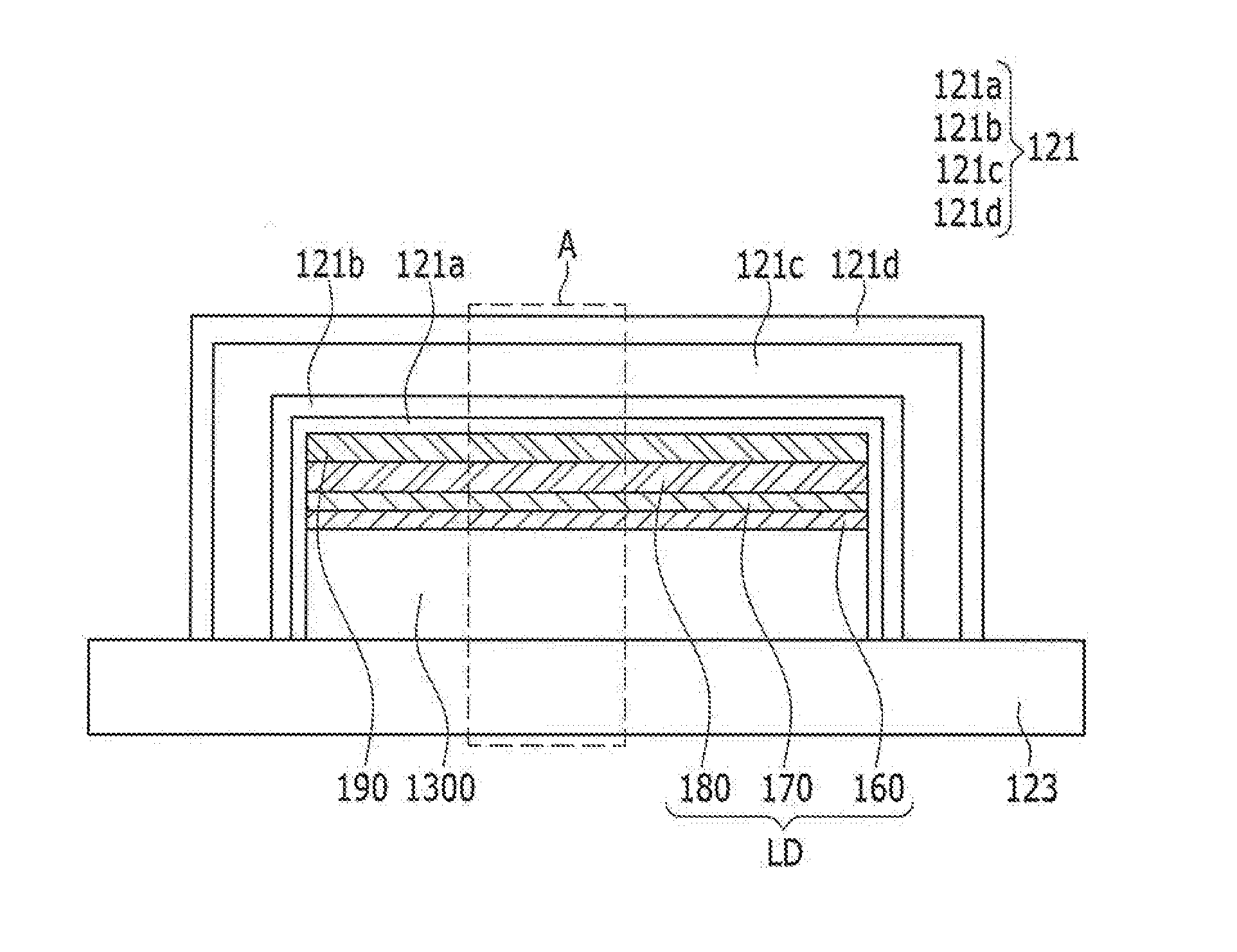
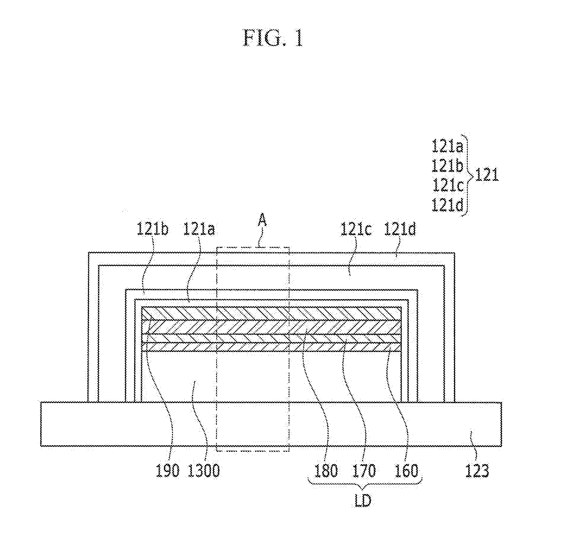
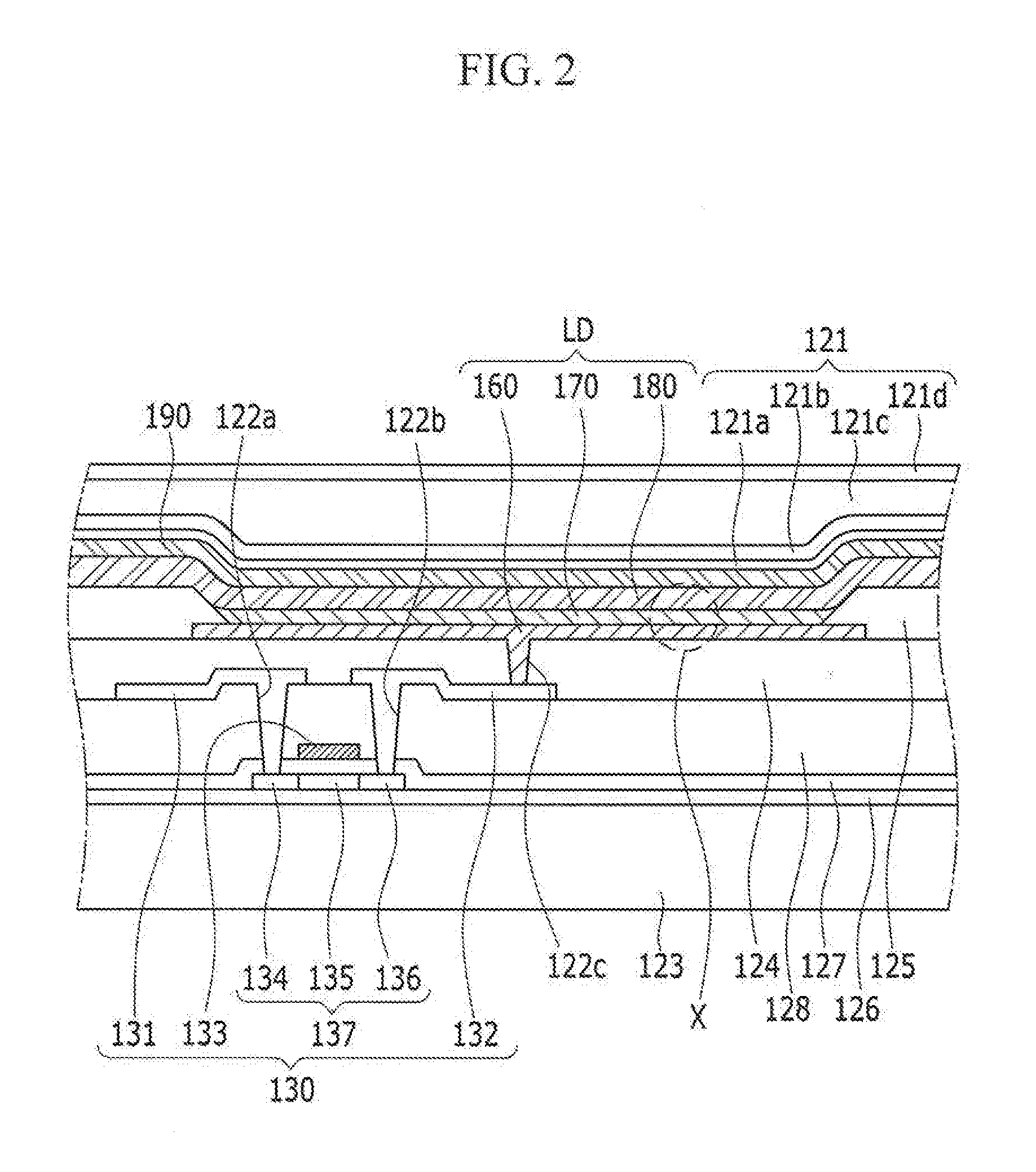
[0039]FIG. 1 illustrates a cross-section...


PUM


Abstract

An organic light emitting diode display including: a substrate; an organic light emitting diode on the substrate; a capping layer on the organic light emitting diode and including a high refractive layer including an inorganic material having a refractive index that is equal to or greater than about 1.7 and equal to or less than about 6.0; and a thin film encapsulation layer covering the capping layer and the organic light emitting diode, the inorganic material including at least one selected from the group consisting of CuI, thallium iodide (TlI), BaS, Cu2O, CuO, BiI, WO3, TiO2, AgI, CdI2, HgI2, SnI2, PbI2, BiI3, ZnI2, MoO3, Ag2O, CdO, CoO, Pr2O3, SnS, PbS, CdS, CaS, ZnS, ZnTe, PbTe, CdTe, SnSe, PbSe, CdSe, AlAs, GaAs, InAs, GaP, InP, AlP, AlSb, GaSb, and InSb.

Description

CROSS-REFERENCE TO RELATED APPLICATION[0001]This application claims priority to and the benefit of Korean Patent Application No. 10-2015-0090722, filed on Jun. 25, 2015 in the Korean Intellectual Property Office, the entire content of which is incorporated herein by reference.BACKGROUND[0002]1. Field[0003]Aspects of embodiments of the present disclosure relate to an organic light emitting diode display.[0004]2. Description of the Related Art[0005]The recent trend toward lightweight and thin personal computers and television sets necessitates lightweight and thin display devices, and flat panel displays (e.g., a liquid crystal display (LCD)) satisfying such requirements are being substituted for conventional cathode ray tubes (CRTs). However, since an LCD is a passive display device, an additional backlight is needed as a light source, and LCDs have various problems, such as a slow response time and a narrow viewing angle.[0006]In this regard, an organic light emitting diode (OLED) d...

Claims


Application Information

Patent Timeline
Patent Type & Authority Applications(United States)
IPC IPC(8): H01L51/52H01L51/50H10K99/00
CPCH01L51/5256H01L51/5218H01L51/5036H01L51/5028H01L51/0072H01L51/0061H01L51/0073H01L51/0074H01L2251/301H10K85/00H10K50/11H10K59/8731H10K59/873H10K59/879H10K59/875H10K59/876H10K59/35H10K85/636H10K85/6576H10K85/6574H10K85/6572H10K2102/3026H10K50/858H10K50/85H10K50/00H10K50/844H10K50/852H10K50/8445
Inventor KIM, WON JONGKIM, DONG CHANKIM, EUNG DOSEO, DONG KYUIM, DA HEAYIM, SANG HOONCHO, YOON HYEUNGHAN, WON SUK
Owner SAMSUNG DISPLAY CO LTD
Learn More