Reducing Autodoping of III-V Semiconductors By Atomic Layer Epitaxy (ALE)

a technology of atomic layer epitaxy and autodoping, which is applied in the direction of single crystal growth, electrical equipment, chemistry apparatus and processes, etc., can solve the problems of difficult prediction of which atoms, difficult ohmic contact to a semiconductor, and difficult to dopant iii-v materials, etc., to achieve the effect of reducing the autodoping of iii-v semiconductor materials

Inactive Publication Date: 2017-01-05
ELPIS TECH INC
View PDF4 Cites 6 Cited by
  • Summary
  • Abstract
  • Description
  • Claims
  • Application Information

AI Technical Summary

Problems solved by technology

Making an Ohmic contact to a semiconductor can be challenging.
Doping of III-V materials can, however, present some notable challenges.
However, since III-V materials contain both group III and group V elements, it is not always easy to predict which atoms (group III or group V) the dopant will replace.

Method used


Image

  • Reducing Autodoping of III-V Semiconductors By Atomic Layer Epitaxy (ALE)
  • Reducing Autodoping of III-V Semiconductors By Atomic Layer Epitaxy (ALE)
  • Reducing Autodoping of III-V Semiconductors By Atomic Layer Epitaxy (ALE)

Examples


Embodiment Construction

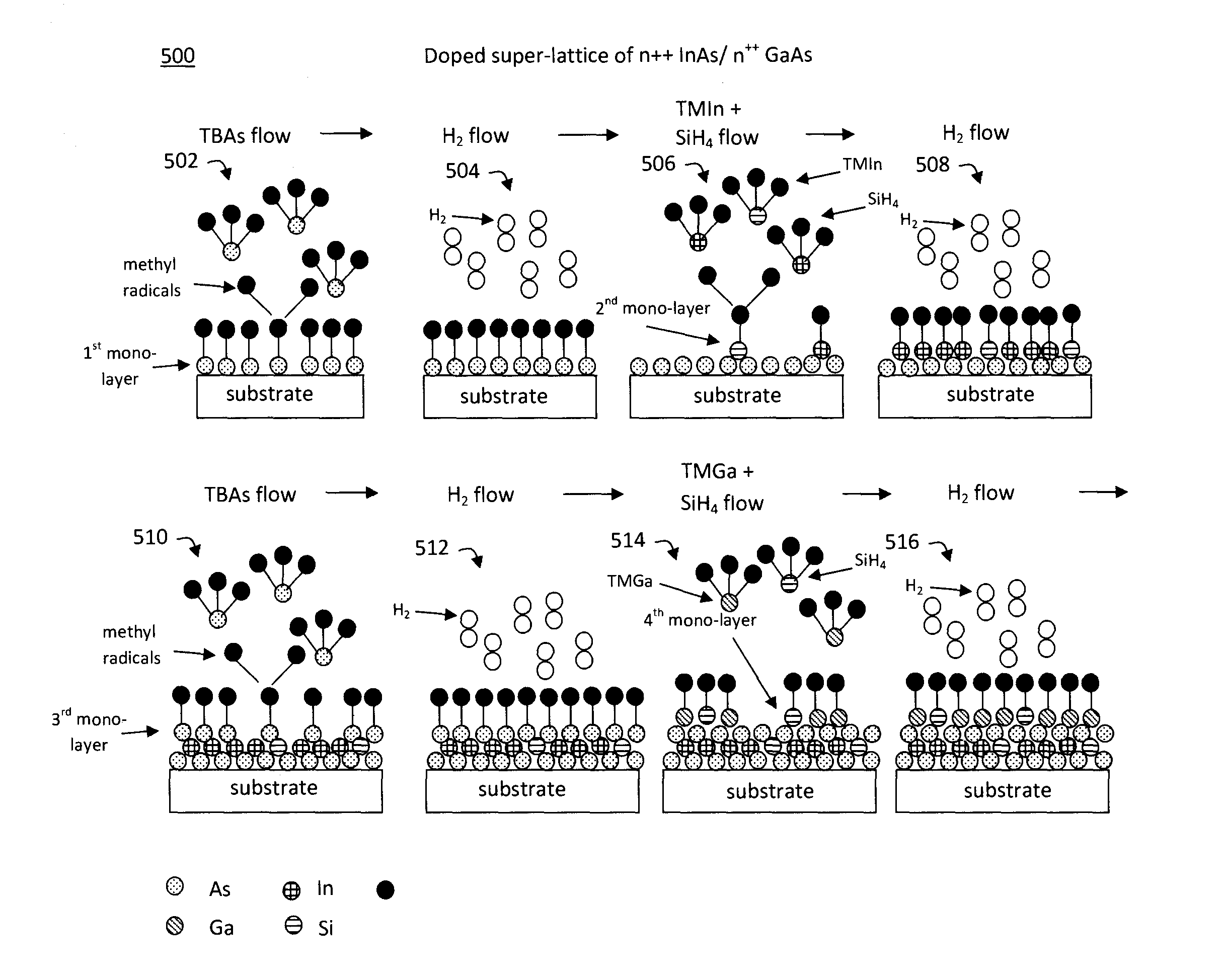
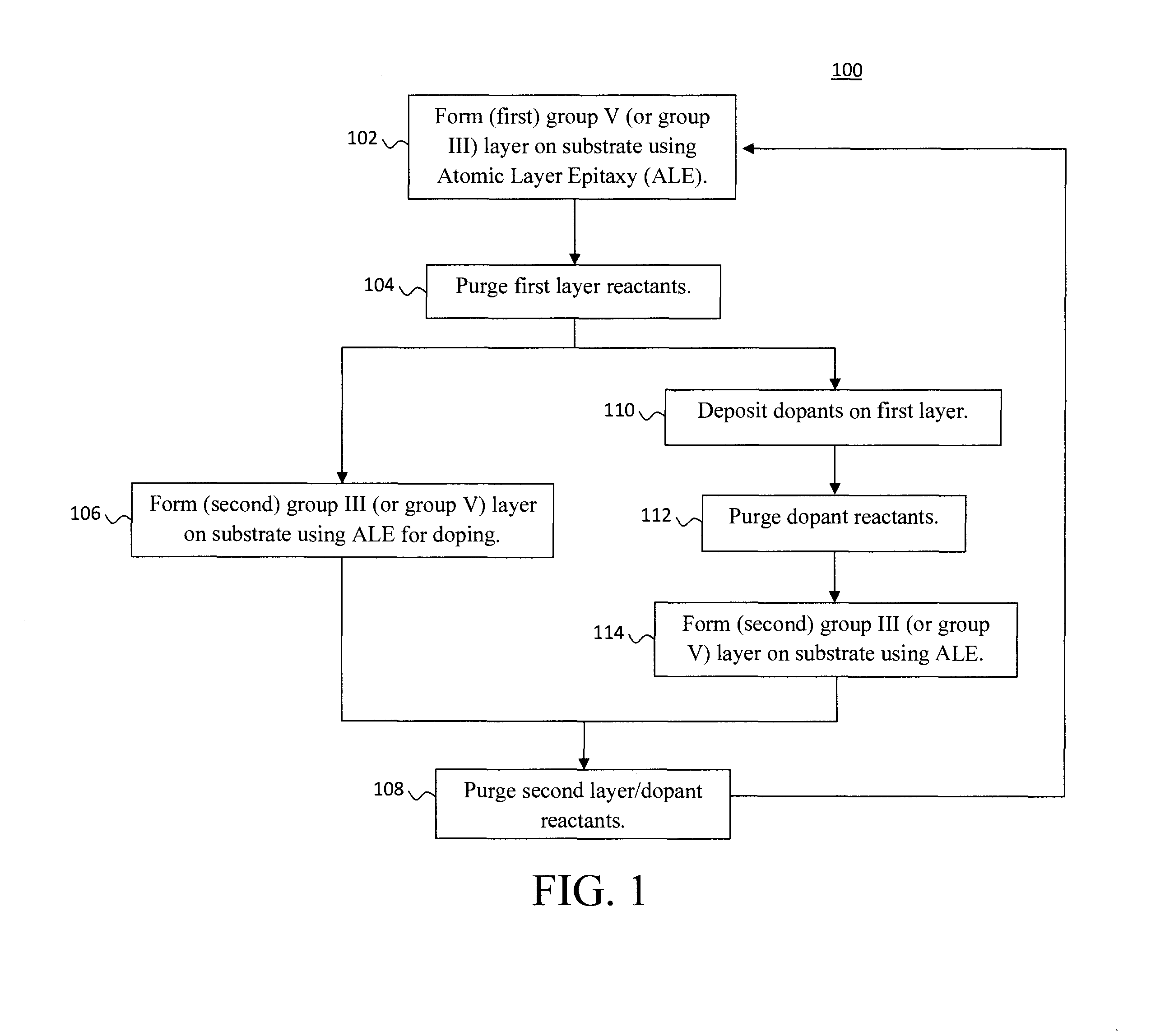
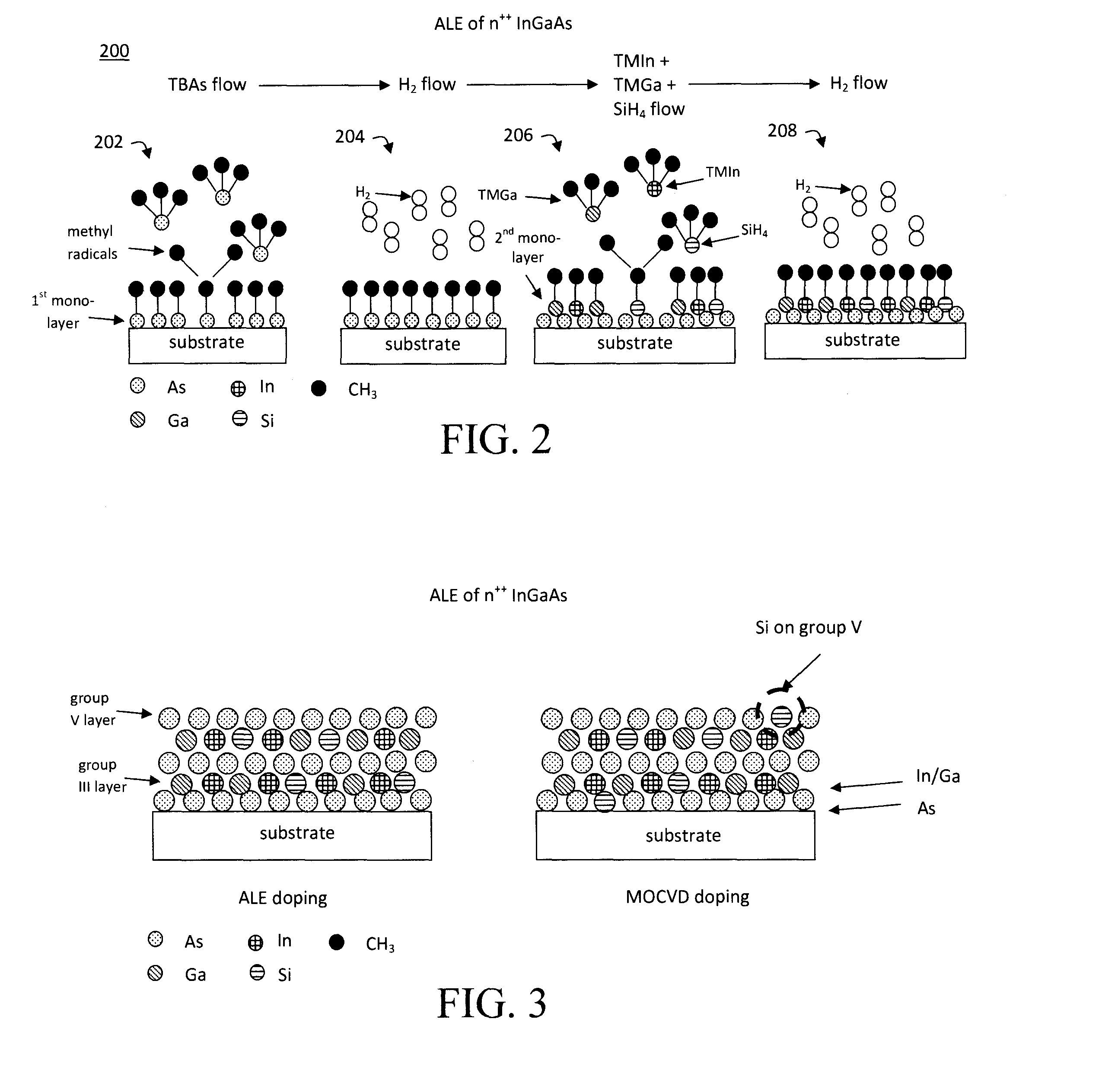
[0015]Provided herein are atomic layer epitaxy (ALE)-based techniques for both forming and in-situ doping a III-V semiconductor material, wherein the III-V semiconductor material is grown layer-by-layer, and wherein the dopant is selectively introduced during (or immediately before) formation of a particular one of the layers for which in-situ doping is desired. As provided above, with amphoteric dopants such as group IV dopants, it can be difficult to control whether the dopant occupies a group-III site or a group-V site since auto-compensation can occur. Advantageously, with the present techniques, the dopant is selectively introduced when there is only either group-III or group-V sites available (but not both) thus effectively forcing the dopant to occupy a particular site, and generally eliminating the possibility for auto-compensation to occur.

[0016]To use a simple example to illustrate this concept, if a layer containing a group V element(s) (a group V layer) is formed separat...


PUM

PropertyMeasurementUnit
temperatureaaaaaaaaaa
carrier concentrationaaaaaaaaaa
free carrier concentrationaaaaaaaaaa

Abstract

In one aspect, a method for forming a doped III-V semiconductor material on a substrate includes the steps of: (a) forming a first monolayer on the substrate, wherein the first monolayer comprises at least one group III or at least one group V element; and (b) forming a doped second monolayer on a side of the first monolayer opposite the substrate, wherein the second monolayer comprises either i) at least one group V element if the first monolayer comprises at least one group III element, or ii) at least one group III element if the first monolayer comprises at least one group V element, wherein a dopant is selectively introduced only during formation of the second monolayer, and wherein steps (a) and (b) are performed using atomic layer epitaxy. Doped III-V semiconductor materials are also provided.

Description

FIELD OF THE INVENTION[0001]The present invention relates to doping of III-V semiconductor materials, and more particularly, to techniques for reducing autodoping of III-V semiconductor materials using atomic layer epitaxy (ALE).BACKGROUND OF THE INVENTION[0002]Making an Ohmic contact to a semiconductor can be challenging. One factor for controlling the contact resistivity is to ensure that the interface (e.g., between the metal and the semiconductor material) is as clean as possible. Thus proper surface cleaning and preparation steps can be implemented prior to depositing the metal over the semiconductor.[0003]Another factor for improving the contact resistivity is to increase the amount of doping in the semiconductor material. Doping can be used to narrow the Schottky barrier that is formed at the metal-semiconductor interface so carriers can tunnel through the barrier. Doping of III-V materials can, however, present some notable challenges. Namely, when doping a III-V material th...

Claims


Application Information

Patent Timeline
Patent Type & Authority Applications(United States)
IPC IPC(8): H01L21/02C30B29/40C30B25/14
CPCH01L21/02546C30B25/165C30B29/40H01L21/02392H01L21/0254H01L21/02543H01L21/02549H01L21/02576H01L21/02579H01L21/0262
Inventor COHEN, GUY M.LAVOIE, CHRISTIAN
Owner ELPIS TECH INC
Why Eureka
Try Eureka