Multiple beam additive manufacturing

a technology of additive manufacturing and beams, applied in the direction of additive manufacturing processes, manufacturing tools, welding/soldering/cutting articles, etc., can solve the problems of slow build rate and manufacturing speed, stress being created in the fused material of each build layer, and the failure of lam techniques

Inactive Publication Date: 2017-01-26
IPG PHOTONICS CORP
View PDF8 Cites 175 Cited by
  • Summary
  • Abstract
  • Description
  • Claims
  • Application Information

AI Technical Summary

Problems solved by technology

Although such laser additive manufacturing (LAM) techniques have been successful, the movement of the laser to the selected regions often slows the build rate and the speed of manufacturing.
Multiple beams have been used in an effort to increase speeds, but scanning multiple beams across the powder layers may result in stresses being created in the fused material of each build layer.
As such, LAM techniques have not been as successful when used with certain materials such as superalloys because thermal stresses may result in cracking.
Also, LAM techniques have not been as successful when used with powder material having larger particle sizes because the power of the laser may not be sufficient to melt and fuse larger particles sizes without causing excessive thermal stress.
Increasing the power of a LAM system is challenging because optical elements must be larger and cooling must be increased to withstand the higher power.
The scanning mirror in such systems becomes less responsive with the increased size, which decreases the scanning speed and reduces build speed.
Attempts at using multiple beams in SLM systems have been unsuccessful because of the challenges involved with scanning the same area with multiple beams.

Method used


Image

  • Multiple beam additive manufacturing
  • Multiple beam additive manufacturing
  • Multiple beam additive manufacturing

Examples


Embodiment Construction

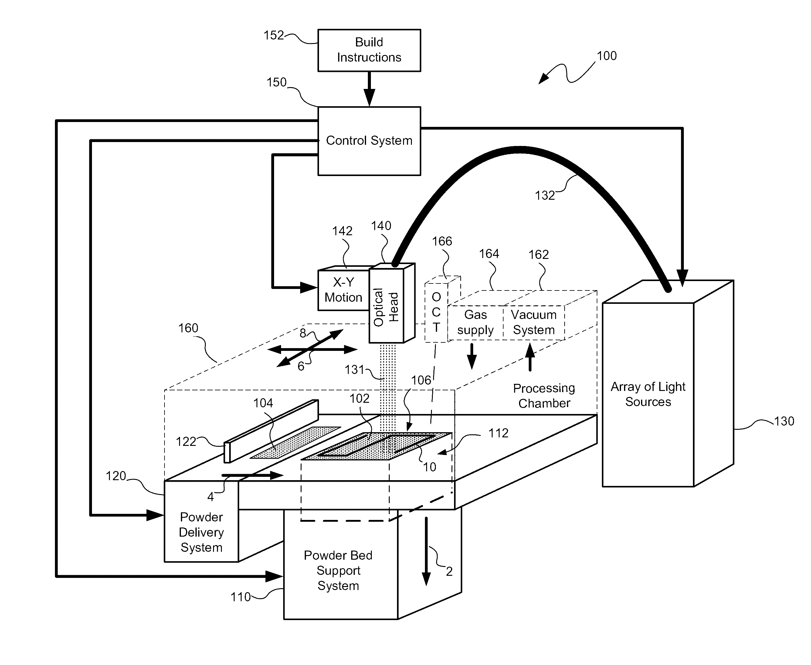
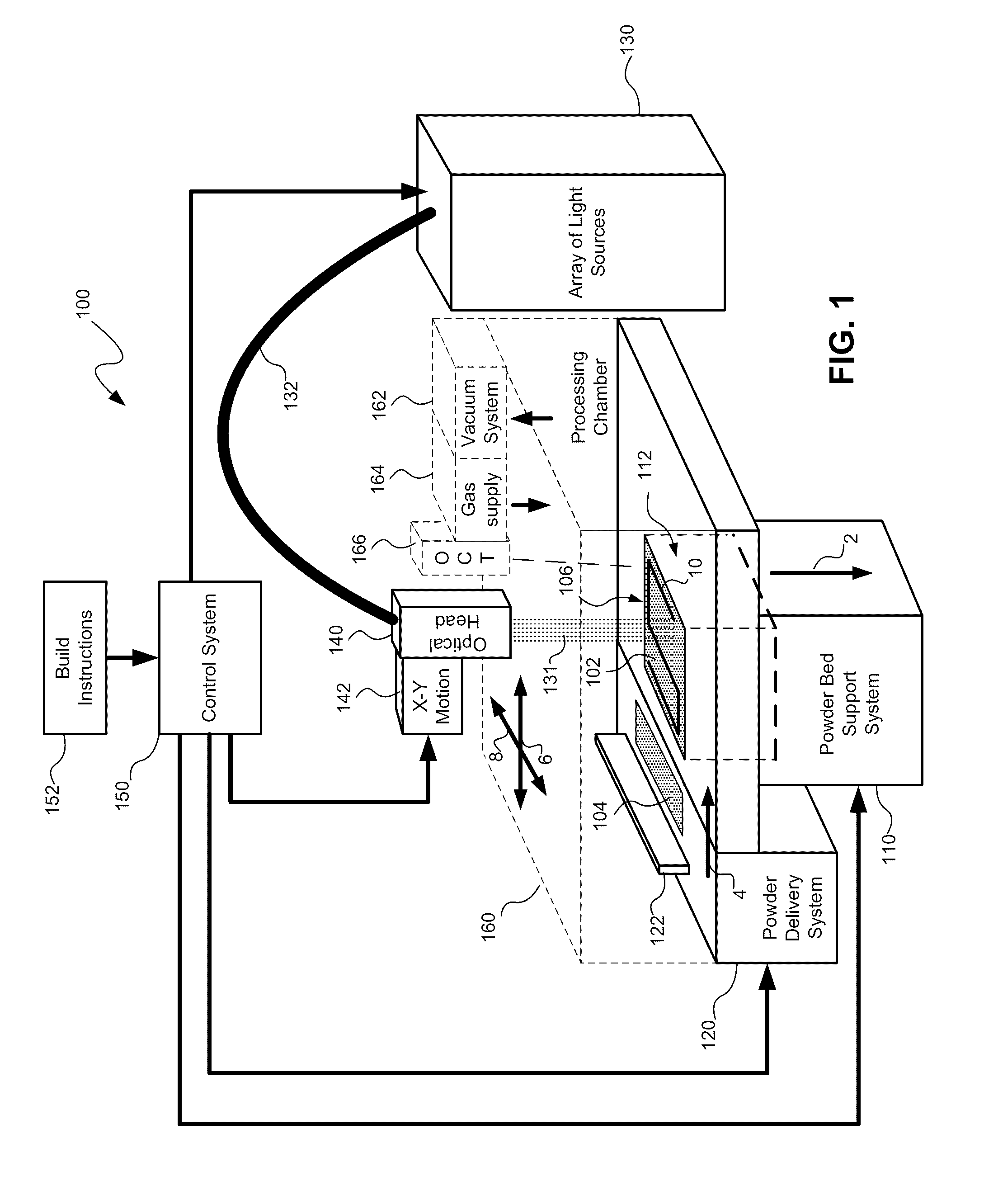
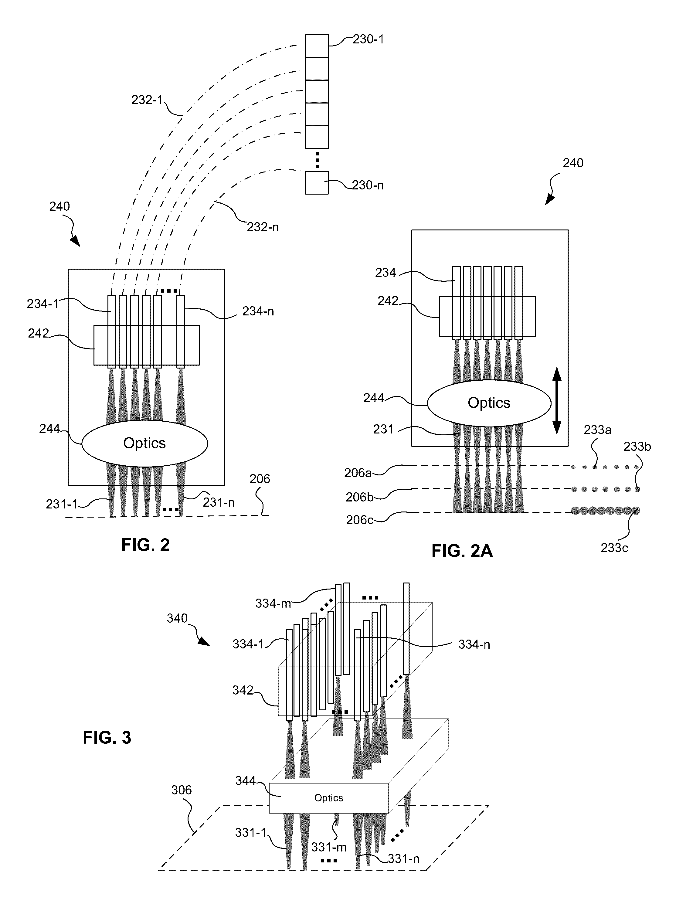
[0040]Systems and methods for multiple beam additive manufacturing, consistent with the present disclosure, use multiple beams of light (e.g., laser light) to expose layers of powder material in selected regions until the powder material fuses to form voxels, which form build layers of a three-dimensional structure. The light may be generated from selected light sources and coupled into an array of optical fibers having output ends arranged in an optical head in at least one line such that multiple beams are sequentially directed by the optical head to the same powder region providing multiple beam sequential exposures (e.g., with pre-heating, melting and controlled cool down) to fuse the powder region. The multiple sequential beams may be moved using various techniques (e.g., by moving the optical head) and according to various scan patterns such that a plurality of fused regions form each build layer.

[0041]By providing multiple beam sequential exposures with varying intensity over...


PUM

PropertyMeasurementUnit
sizeaaaaaaaaaa
sizeaaaaaaaaaa
particle sizesaaaaaaaaaa

Abstract

Systems and methods for multiple beam additive manufacturing use multiple beams of light (e.g., laser light) to expose layers of powder material in selected regions until the powder material fuses to form voxels, which form build layers of a three-dimensional structure. The light may be generated from selected light sources and coupled into an array of optical fibers having output ends arranged in an optical head in at least one line such that multiple beams are sequentially directed by the optical head to the same powder region providing multiple beam sequential exposures (e.g., with pre-heating, melting and controlled cool down) to fuse the powder region. The multiple sequential beams may be moved using various techniques (e.g., by moving the optical head) and according to various scan patterns such that a plurality of fused regions form each build layer.

Description

CROSS-REFERENCE TO RELATED APPLICATIONS[0001]The present application claims the benefit of U.S. Patent Application Ser. No. 62 / 173,541 filed Jun. 10, 2015, which is fully incorporated herein by reference.BACKGROUND OF THE DISCLOSURE[0002]Field of the Disclosure[0003]The present disclosure relates to additive manufacturing and more particularly, to multiple beam additive manufacturing.[0004]Background Art Discussion[0005]Additive manufacturing (also known as three-dimensional printing) techniques have been used to manufacture three-dimensional structures of almost any shape. Using an additive process, successive layers of material are deposited to form the structure based on data defining a 3D model of the structure. In some methods, referred to as powder bed fusion (PBF), the successive layers forming the structure are produced by depositing successive layers of powder material and using a light beam (e.g., laser light) to bind or fuse the powder material in selected regions of each...

Claims


Application Information

Patent Timeline
Patent Type & Authority Applications(United States)
IPC IPC(8): B23K26/342B33Y30/00B23K26/073B23K26/06B23K26/082B33Y10/00B33Y50/02
CPCB23K26/342B33Y10/00B33Y30/00B33Y50/02B23K2203/08B23K26/082B23K26/073B23K26/0626B23K26/0604B29C64/153B23K2103/08B29C64/277B29C64/268Y02P10/25B22F10/28B22F10/366B22F12/45B22F12/47B22F2999/00B22F12/41B22F10/36B22F12/49B22F12/52B23K26/0869B33Y70/10B29C64/386
Inventor DALLAROSA, JOSEPHO'NEILL, WILLIAMSQUIRES, DAVIDSPARKES, MARTINPAYNE, ANDREW
Owner IPG PHOTONICS CORP
Why Eureka
Try Eureka