Method of Patterning Without Dummy Gates

Active Publication Date: 2017-02-09
TOKYO ELECTRON LTD
View PDF4 Cites 15 Cited by
  • Summary
  • Abstract
  • Description
  • Claims
  • Application Information

AI Technical Summary

Benefits of technology

[0007]Techniques herein provide precise cuts for fins and nanowires without needing dummy gate pairs to ensure accuracy. Techniques herein include leaving fins uncut until gates are opened, and then one opened gate structure is used to focus placement of cuts. Surrounding dielectric material is used as part of an etch mask to ensure cuts happen at specified locations. With etch selectivity to gate spacer material, uncovered fins—further defined by an etch mask formed thereon—can be etched inside/within a space formerly occupied by a gate structure. After etching the uncovered fins, the s

Problems solved by technology

Cutting such relatively small features can be problematic because etch masks created by photolithographic systems do not have sufficient resolution to accurately cut or remove material within specified tolerances.
Using such conventional etch masks can result in device poor device performance or device failure.
Thus, a fin is formed and then two dummy gates are used to cut fins because at conventional small patterning scales t

Method used


Image

  • Method of Patterning Without Dummy Gates
  • Method of Patterning Without Dummy Gates
  • Method of Patterning Without Dummy Gates

Examples


Embodiment Construction

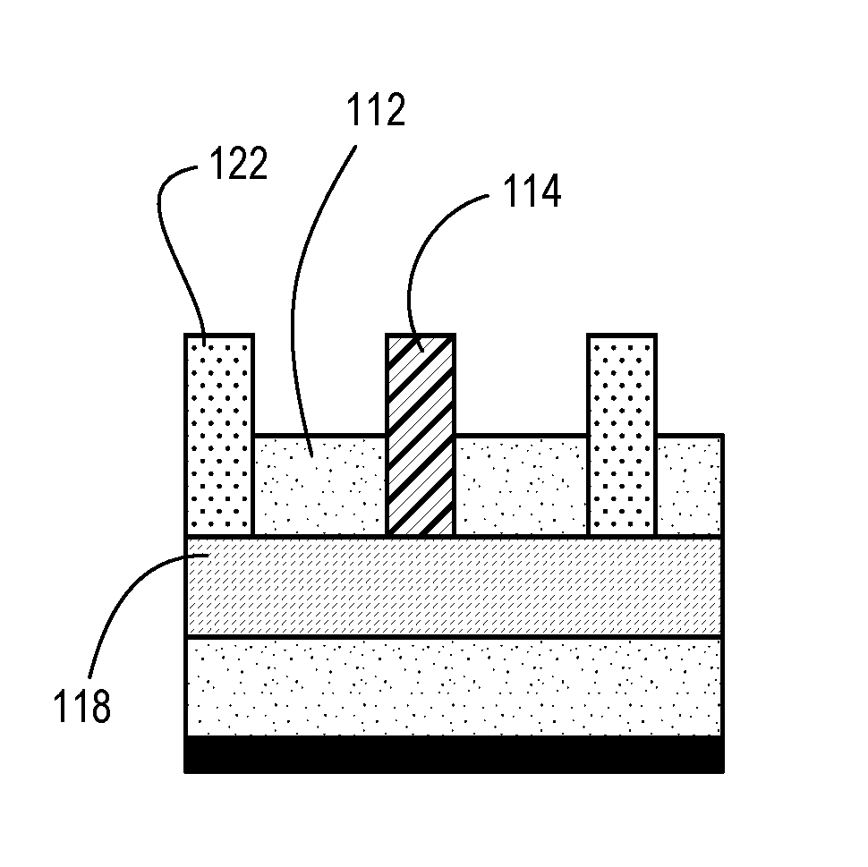
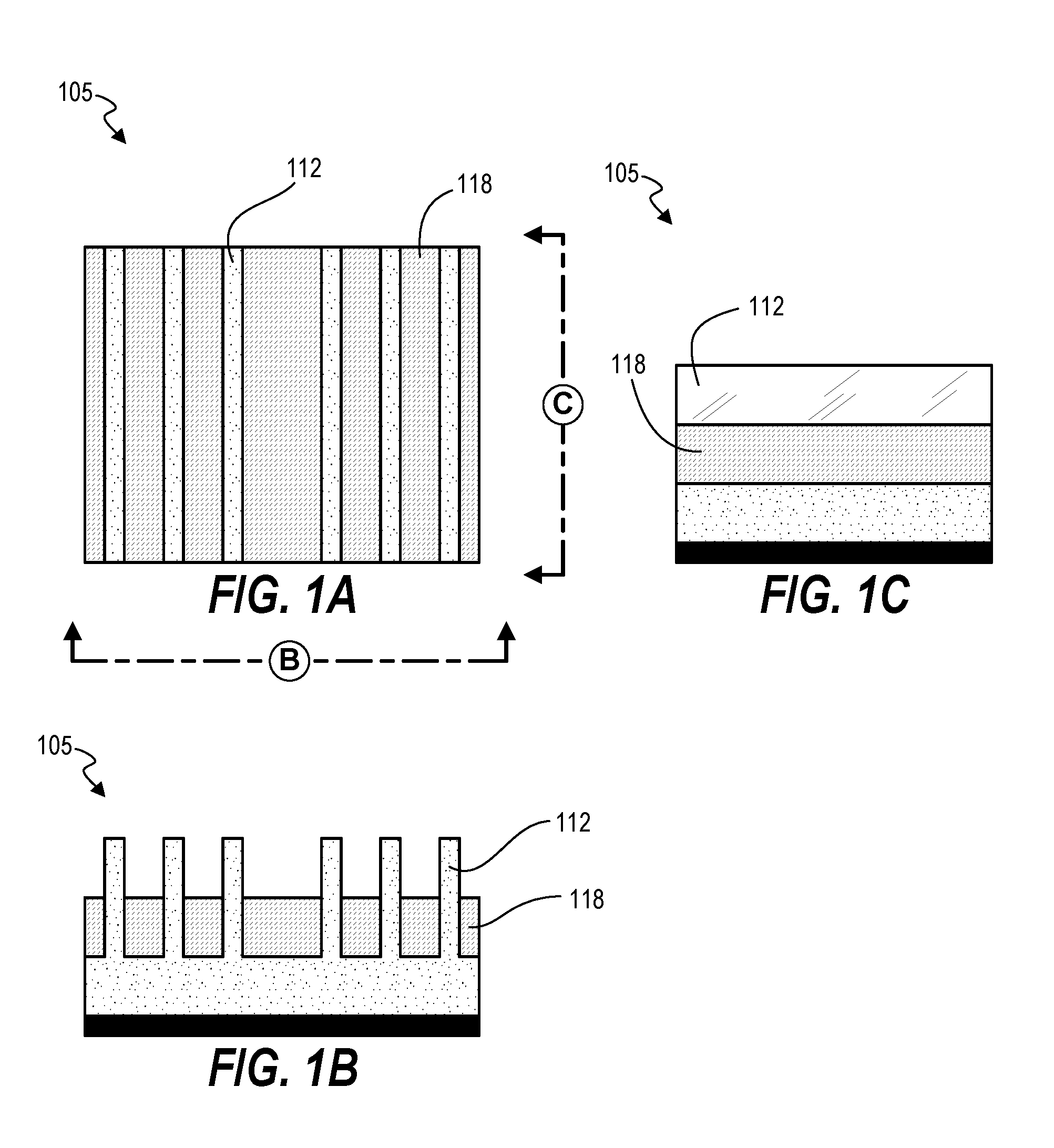
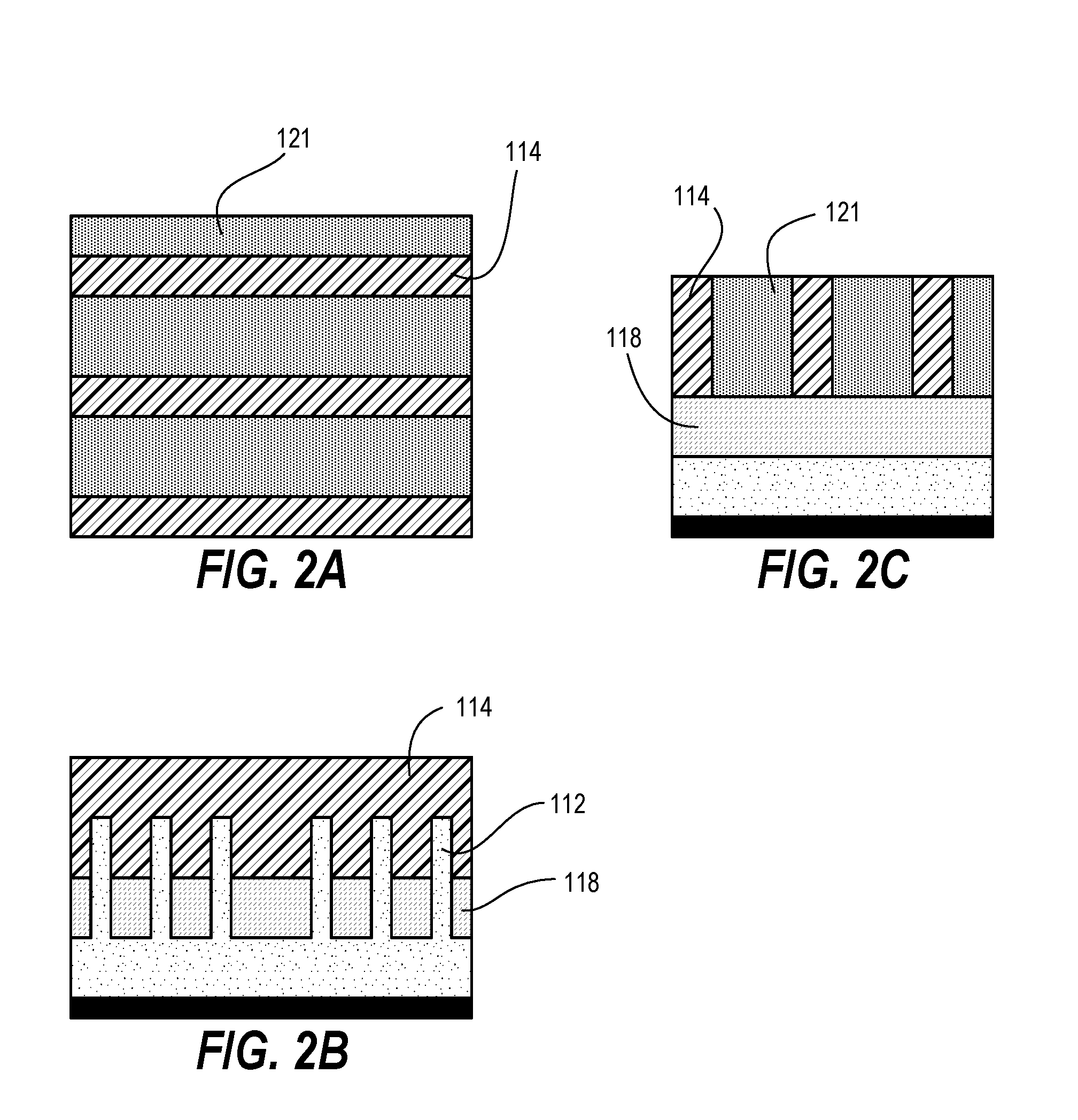
[0035]Techniques herein provide precise cuts for fins and nanowires without needing dummy gate pairs to ensure accuracy. Techniques herein include leaving fins uncut until gates are opened, and then one opened gate structure is used to focus placement of cuts. Surrounding dielectric material is used as part of an etch mask to ensure cuts happen at specified locations. With etch selectivity to gate spacer material, uncovered fins—further defined by an etch mask formed thereon—can be etched inside / within a space formerly occupied by a gate structure. After etching the uncovered fins, the space can be filled with dielectric material. Such filler dielectric material can remain in place which results in the space formerly occupied by the gate structure does not become metallized but remains as a dielectric. This means that there are no metallized dummy gates left on the device, and that pairs of dummy gates are not needed to be designed into the cell. Accordingly, with techniques herein,...


PUM


Abstract

Techniques herein provide precise cuts for fins and nanowires without needing dummy gate pairs to compensate for overlay misalignment. Techniques herein include using an etch mask to remove designated portions of gate structures to define a trench or open space having fin structures, nanowires, etc. The uncovered fin structures are etched away or otherwise removed from the trench segments. The etch mask and material defining the trench provide a combined etch mask for removing uncovered fin portions. Subsequently the trench segments are filled with dielectric material. Without needed dummy gate pairs a given substrate can fit significantly more electrical devices per unit area.

Description

CROSS REFERENCE TO RELATED APPLICATIONS[0001]The present application claims the benefit of U.S. Provisional Patent Application No. 62 / 202,599, filed on Aug. 7, 2015, entitled “Method of Patterning with Single Diffusion Cuts,” which is incorporated herein by reference in its entirety.BACKGROUND OF THE INVENTION[0002]The present disclosure relates to fabricating semiconductor devices. More particularly, the present disclosure relates to forming and cutting structures such as fins and nanowires.[0003]Transistors, such as field effect transistors (FETs), are the basic elements of microelectronics and integrated circuits. There has been a continuous drive to scale down or shrink transistors and other semiconductor devices to increase density and improve processing performance. Methods of shrinking line-widths in lithographic processes have historically involved using greater-NA optics (numerical aperture), shorter exposure wavelengths, or interfacial media other than air (e.g., water imm...

Claims


Application Information

Patent Timeline
IPC IPC(8): H01L21/027H01L21/28H01L21/02H01L21/3213
CPCH01L21/0274H01L21/32133H01L21/32139H01L21/02603H01L21/28008H01L21/823431H01L29/66795H01L21/0337H01L29/41791H01L29/66621
Inventor SMITH, JEFFREYDEVILLIERS, ANTON J.
Owner TOKYO ELECTRON LTD
Why Eureka
Try Eureka