Circuit probing system and its circuit probing device
a circuit probing and circuit probing technology, which is applied in the direction of printed circuit testing, measurement instrument magnets, instruments, etc., can solve the problems of reducing the pin area deteriorating electrical performance and testing results of the probe card, etc., and enhancing the entire quality testing procedure. , the effect of operator inadvertent touching the probe pin of the probe card
- Summary
- Abstract
- Description
- Claims
- Application Information
AI Technical Summary
Benefits of technology
Problems solved by technology
Method used
Image

Examples
first embodiment
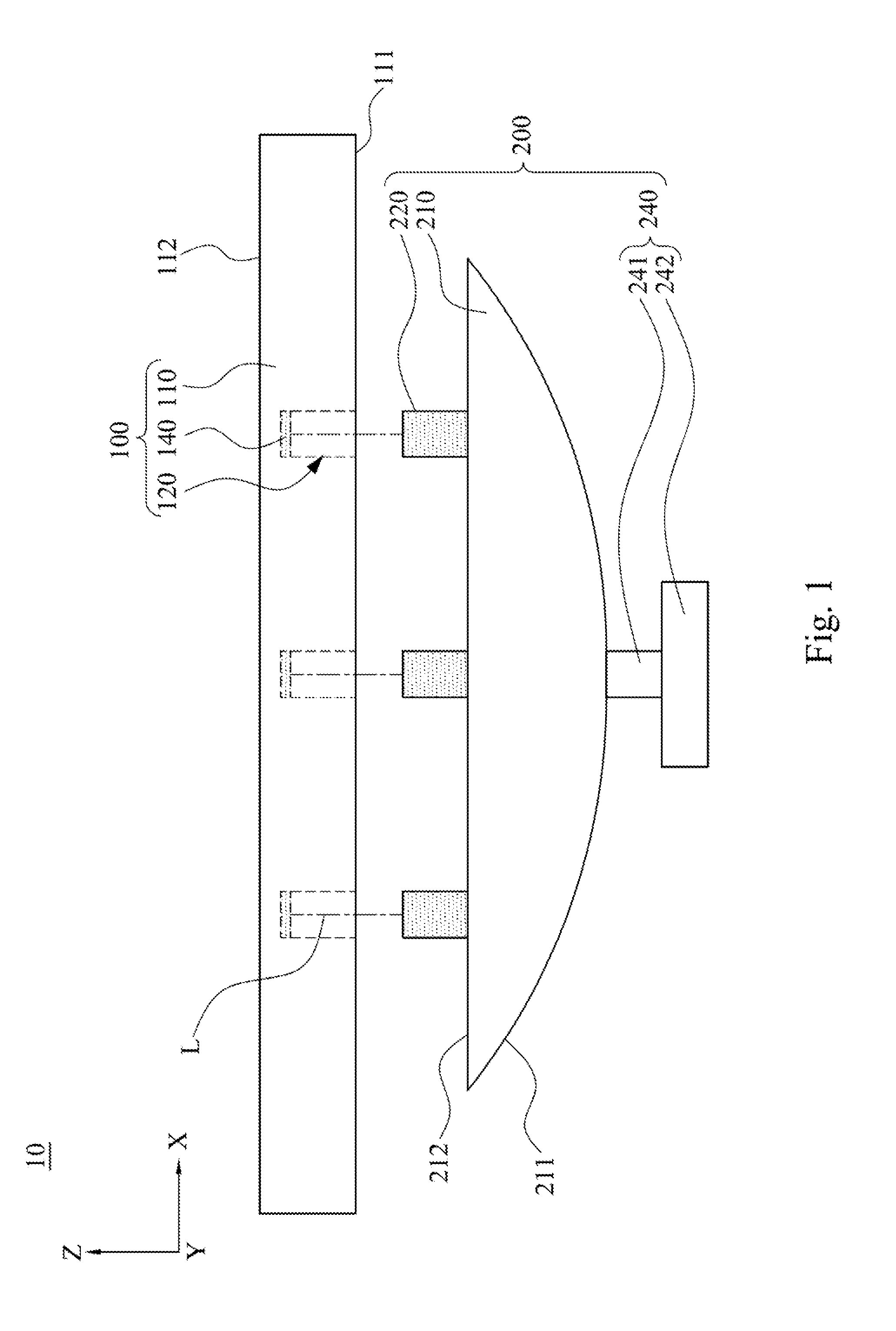
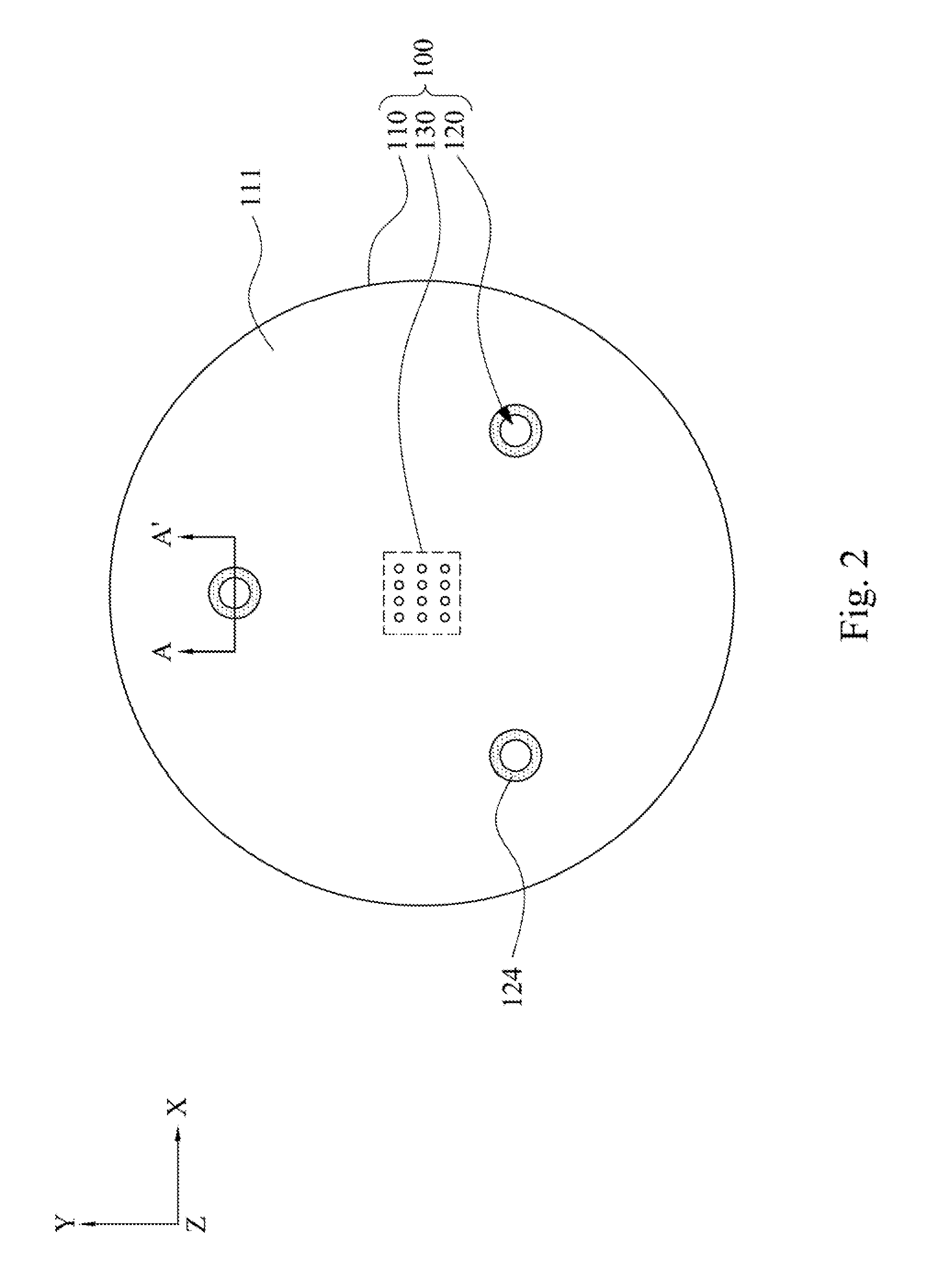
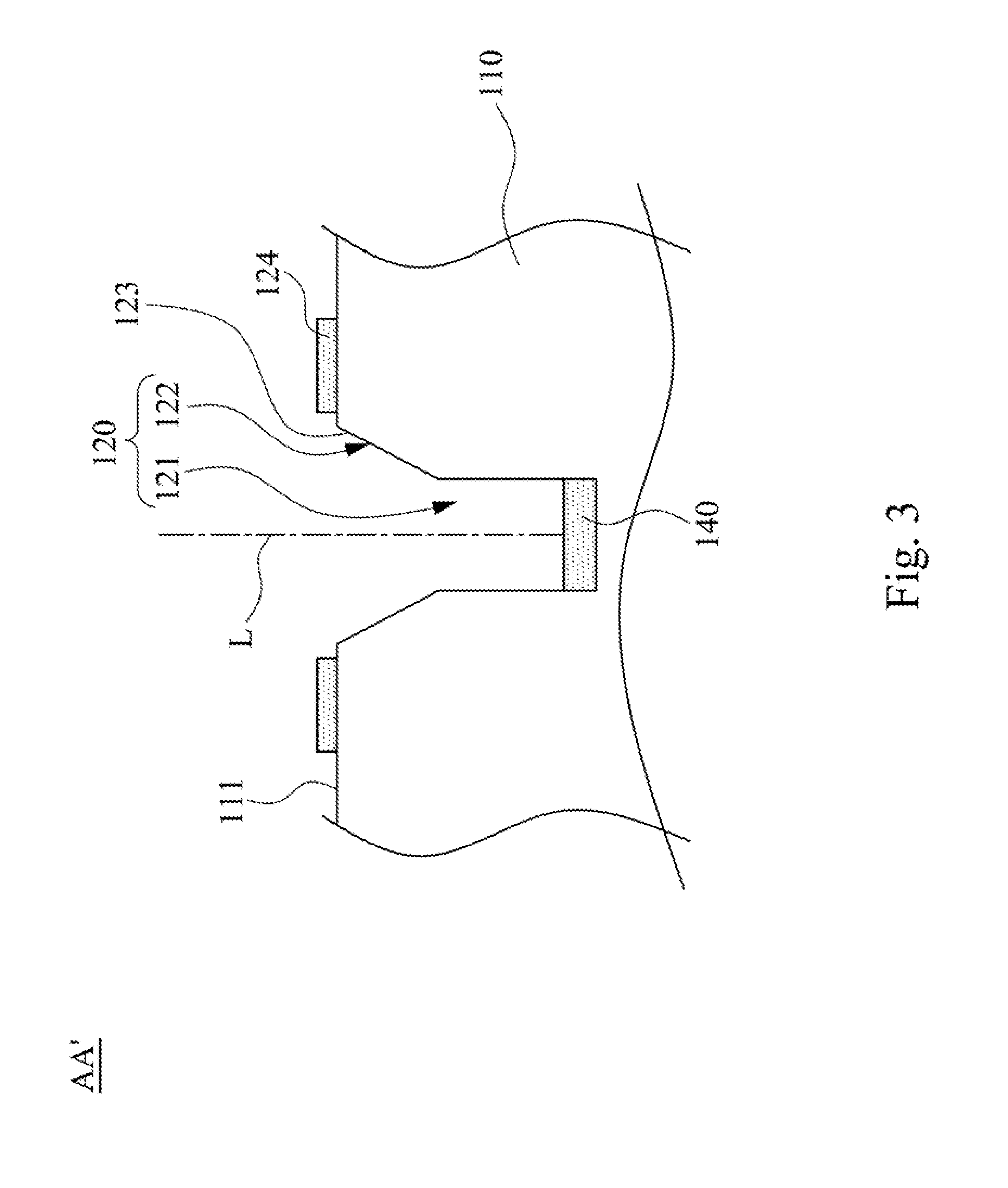
[0035]Reference is now made to FIG. 1 and FIG. 2 in which FIG. 1 is a disassembled view of a probe card 100 and a protective lid 200 of a circuit probing device 10 according to a first embodiment of the disclosure. FIG. 2 is a top view of the probe card 100 of FIG. 1. As shown in FIG. 1 and FIG. 2, the circuit probing device 10 includes a probe card 100 and a protective lid 200. The probe card 100 includes a substrate 110, a pin area 130 and a plurality of first magnetic attraction members 140. The substrate 110 is provided with a front surface 111 and a rear surface 112 opposite to the front surface 111. The pin area 130 is disposed on the front surface 111 of the substrate 110. A plurality of bore holes 120 are respectively formed on the front surface 111 of the substrate 110. Each of the first magnetic attraction members 140 is installed in one of the bore holes 120, and is coupled to the substrate 110. The protective lid 200 is removably fixed to the probe card 100. The protecti...
second embodiment
[0044]The circuit probing device of the second embodiment is substantially the same to the circuit probing device of the first embodiment, except that each of the second magnetic attraction members 220 in the first embodiment (FIG. 1) is made of a magnet (e.g., permanent magnet) completely. In contrast, FIG. 4 is a schematic view of the second magnetic attraction member 230 of the protective lid 201 according to the second embodiment of the disclosure. As shown in FIG. 4, each of the second magnetic attraction members 230 includes a cylindrical body 231 and a magnetic block 232 disposed on one distal end of the cylindrical body 231. The cylindrical body 231 is disposed between the magnetic block 232 and the cover 210 so that the magnetic block 232 can be magnetically attracted with one of the first magnetic attraction members 140.
[0045]Thus, comparing to each of the second magnetic attraction members 220 shown in FIG. 1 made of the magnet (e.g., permanent magnet) completely, a small...
third embodiment
[0046]FIG. 5A-FIG. 5B are operational schematic views of a circuit probing system 1 according to a third embodiment of the disclosure. As shown in FIG. 5A-FIG. 5B, in this embodiment, the circuit probing system 1 includes the aforementioned circuit probing device 10, an object-removing device 300 and a transmission device 400. All features of the circuit probing device 10 of the aforementioned embodiments can be adapted to the circuit probing device 10 of the third embodiment. The object-removing device 300 linearly removes the protective lid 200 away from the probe card 100 in a second direction (i.e., Z axis downward) by moving the grip portion 240. The transmission device 400 is electrically connected to the object-removing device 300 for driving the object-removing device 300 to move. The transmission device 400, for example, can be a motor, a cylinder or other conventional techniques, however, the disclosure is not limited thereto, one skilled in the art of the disclosure may b...
PUM
 Abstract
Description
Claims
Application Information
 - R&D
- Intellectual Property
- Life Sciences
- Materials
- Tech Scout
- Unparalleled Data Quality
- Higher Quality Content
- 60% Fewer Hallucinations
Browse by: Latest US Patents, China's latest patents, Technical Efficacy Thesaurus, Application Domain, Technology Topic, Popular Technical Reports.
© 2025 PatSnap. All rights reserved.Legal|Privacy policy|Modern Slavery Act Transparency Statement|Sitemap|About US| Contact US: help@patsnap.com