

Semiconductor modification process and structures
- Summary
- Abstract
- Description
- Claims
- Application Information
AI Technical Summary
Benefits of technology
Problems solved by technology
Method used
Image

Examples
Example
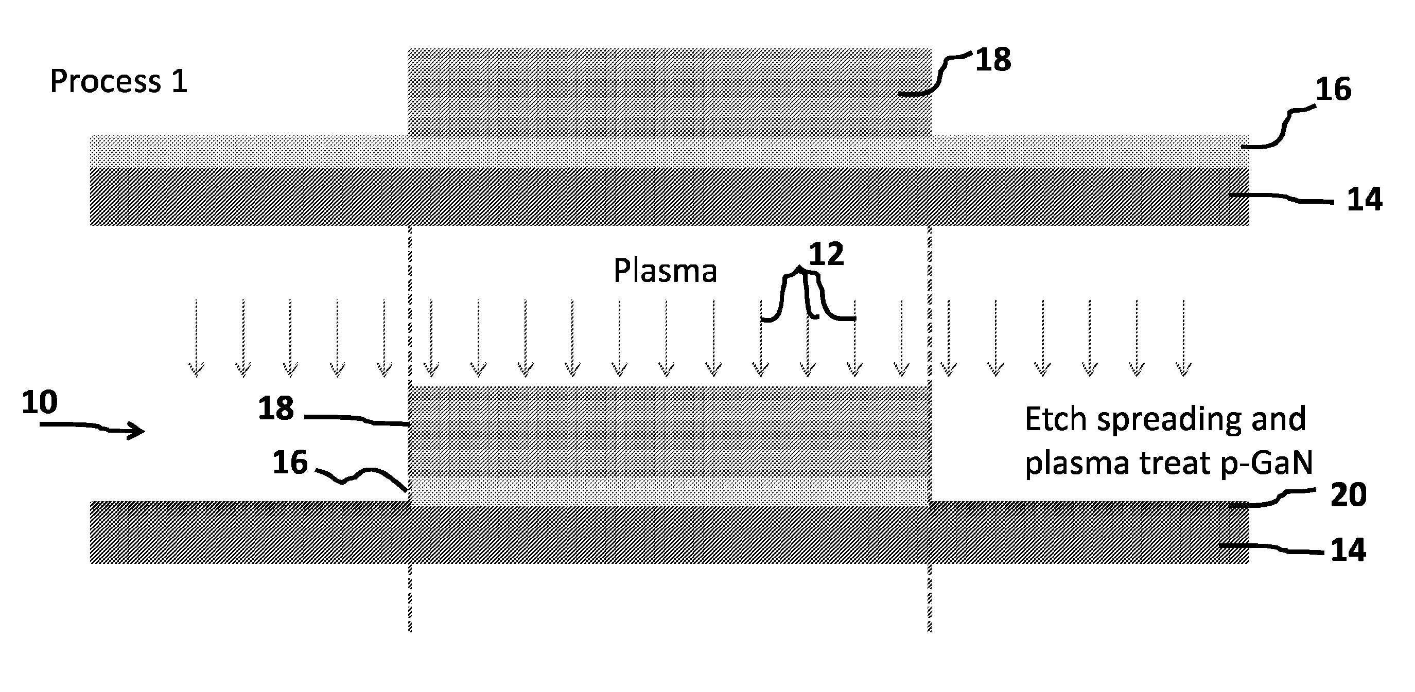
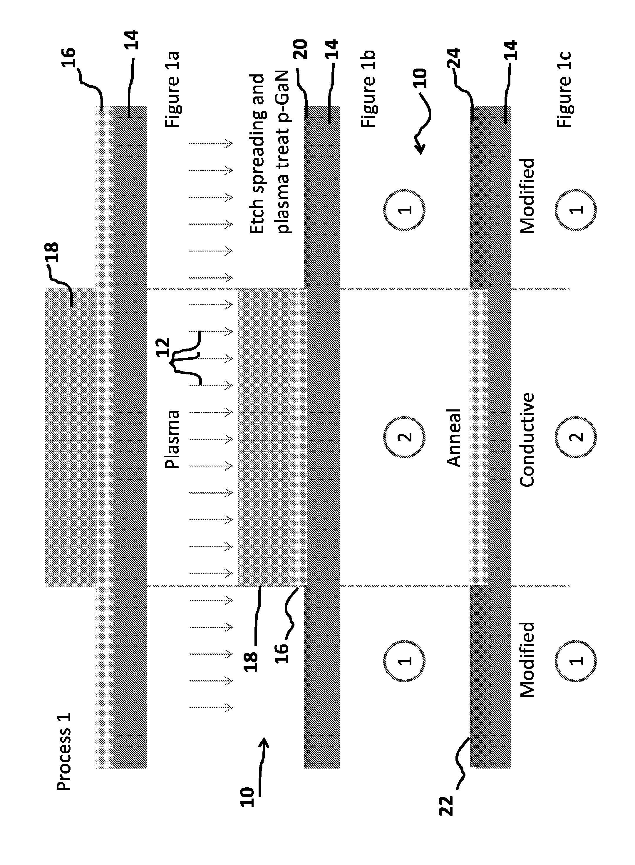
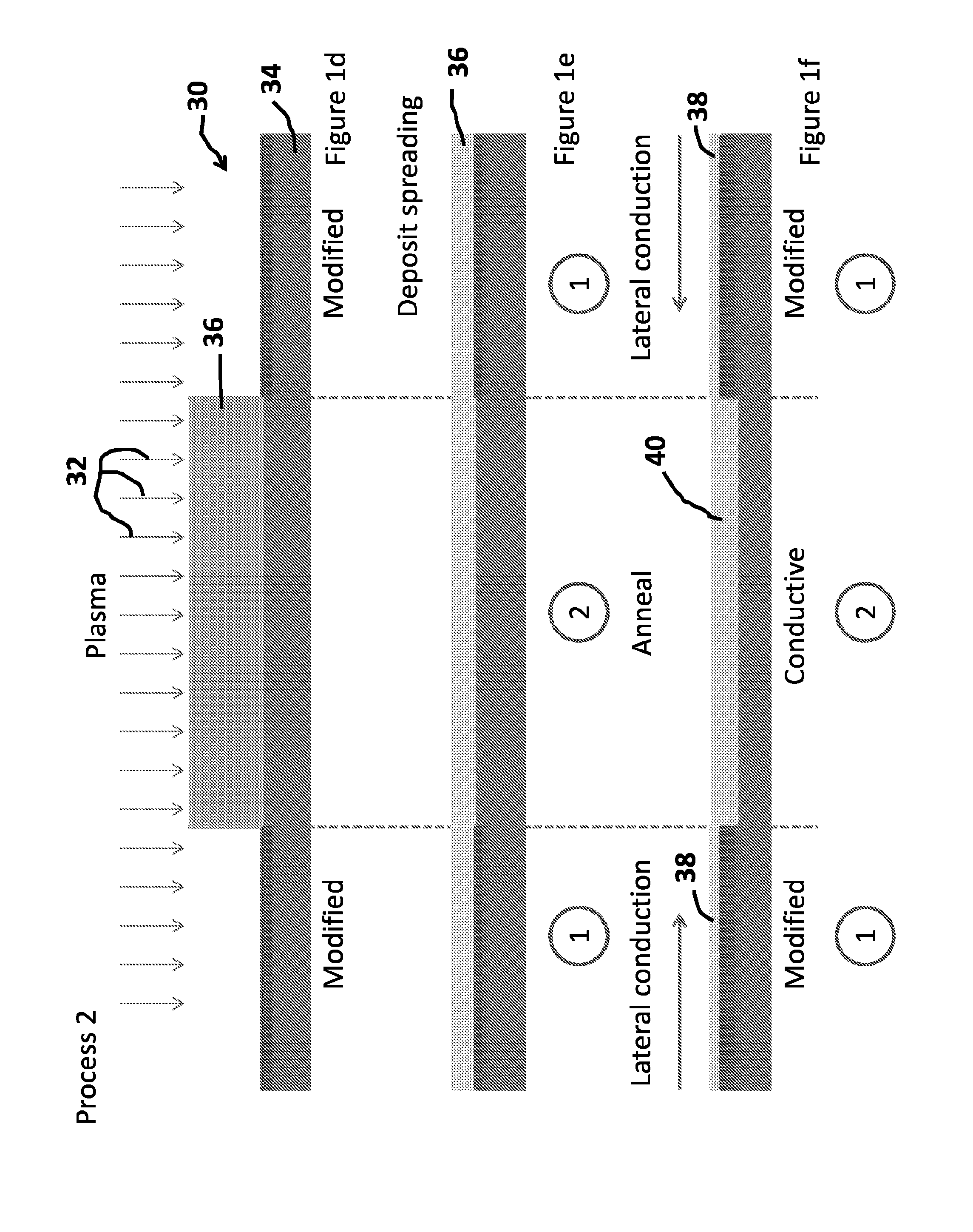
[0107]Generally speaking, the present invention resides in the provision of providing improved device performance and fabrication techniques for semiconductors e.g. GaN semiconductors.
[0108]Although plasma treatment is known to reduce LED performance an important distinction is the ability and process to selectively modify p-GaN. The present invention focusses on a post-anneal process for forming LED structures which has been found to be critically important for being able to simultaneously form conductive sections and sections which are non-conductive to vertical currents through the p-GaN. In this present plasma and annealing processes described herein (Process 1, 2 and 3) have been developed which enable ohmic and non-conducting to vertical current regions to be formed simultaneously. In particular, the ability to form modified non-conducting to vertical current regions using these processes is innovative and offer many advantages for processing and device formation. The process ...
PUM
 Abstract
Description
Claims
Application Information