Method of manufacturing semiconductor device

Active Publication Date: 2017-02-23
RENESAS ELECTRONICS CORP
View PDF1 Cites 8 Cited by
  • Summary
  • Abstract
  • Description
  • Claims
  • Application Information

AI Technical Summary

Benefits of technology

[0007]When such a non-volatile memory as the add-on circuit is formed in a memory formation region, a well and a gate electrode such as a power transistor are formed in a main circuit formation region, and then, a gate electrode of the non-volatile memory havin

Problems solved by technology

And, when the growth of the crystal grains is promoted, the variation in the resistance difference among the plurality of the resistance elements, that is, deterioration of a so-called mismatch chara

Method used


Image

  • Method of manufacturing semiconductor device
  • Method of manufacturing semiconductor device
  • Method of manufacturing semiconductor device

Examples


embodiment

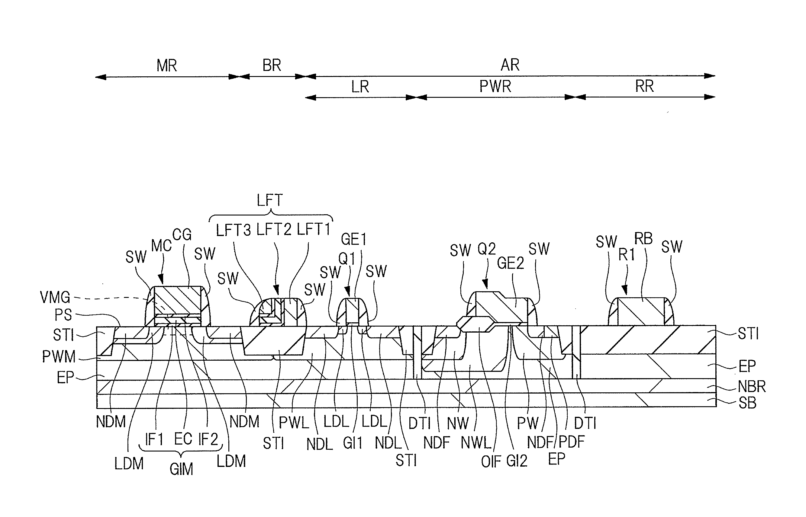
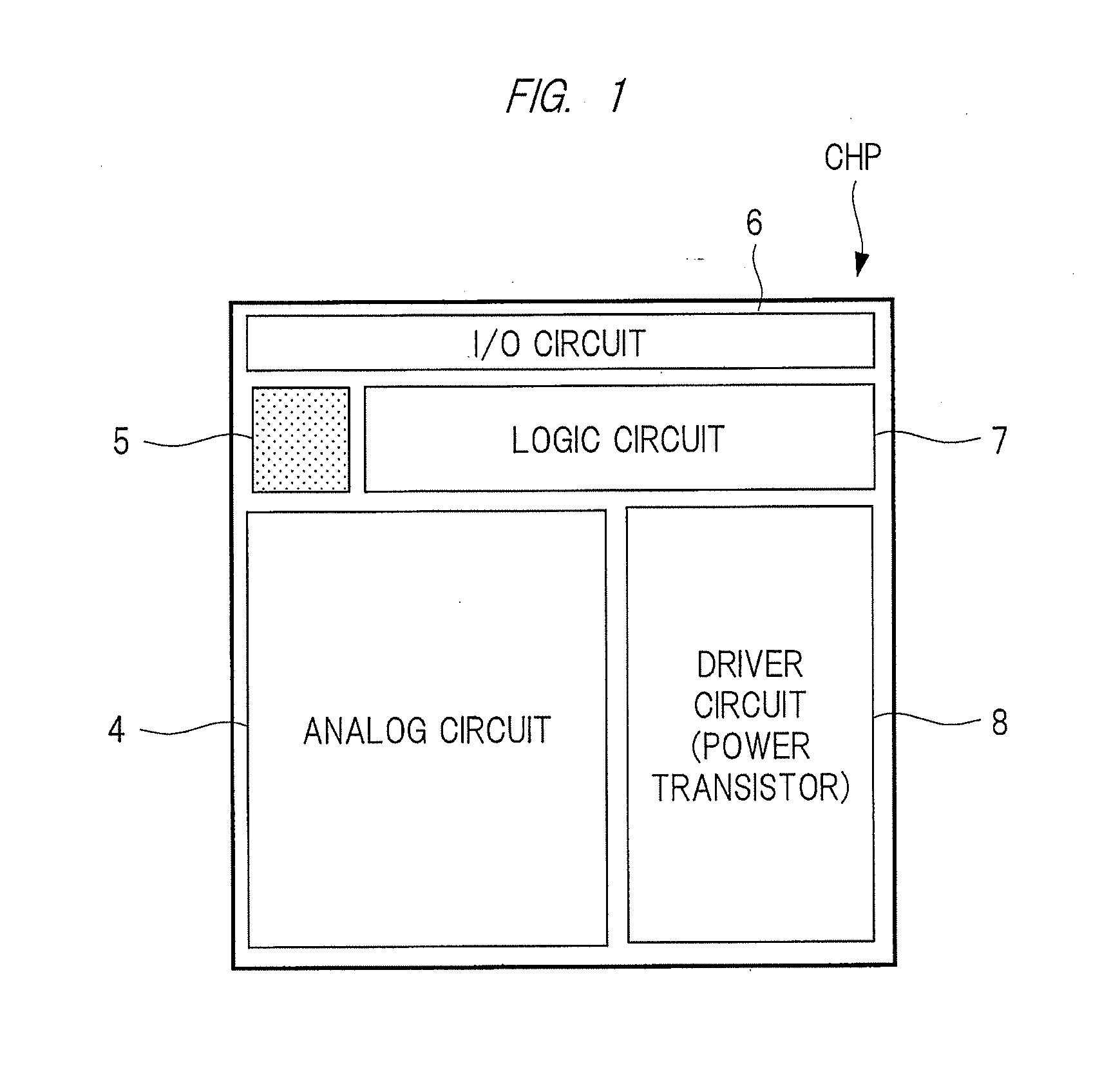
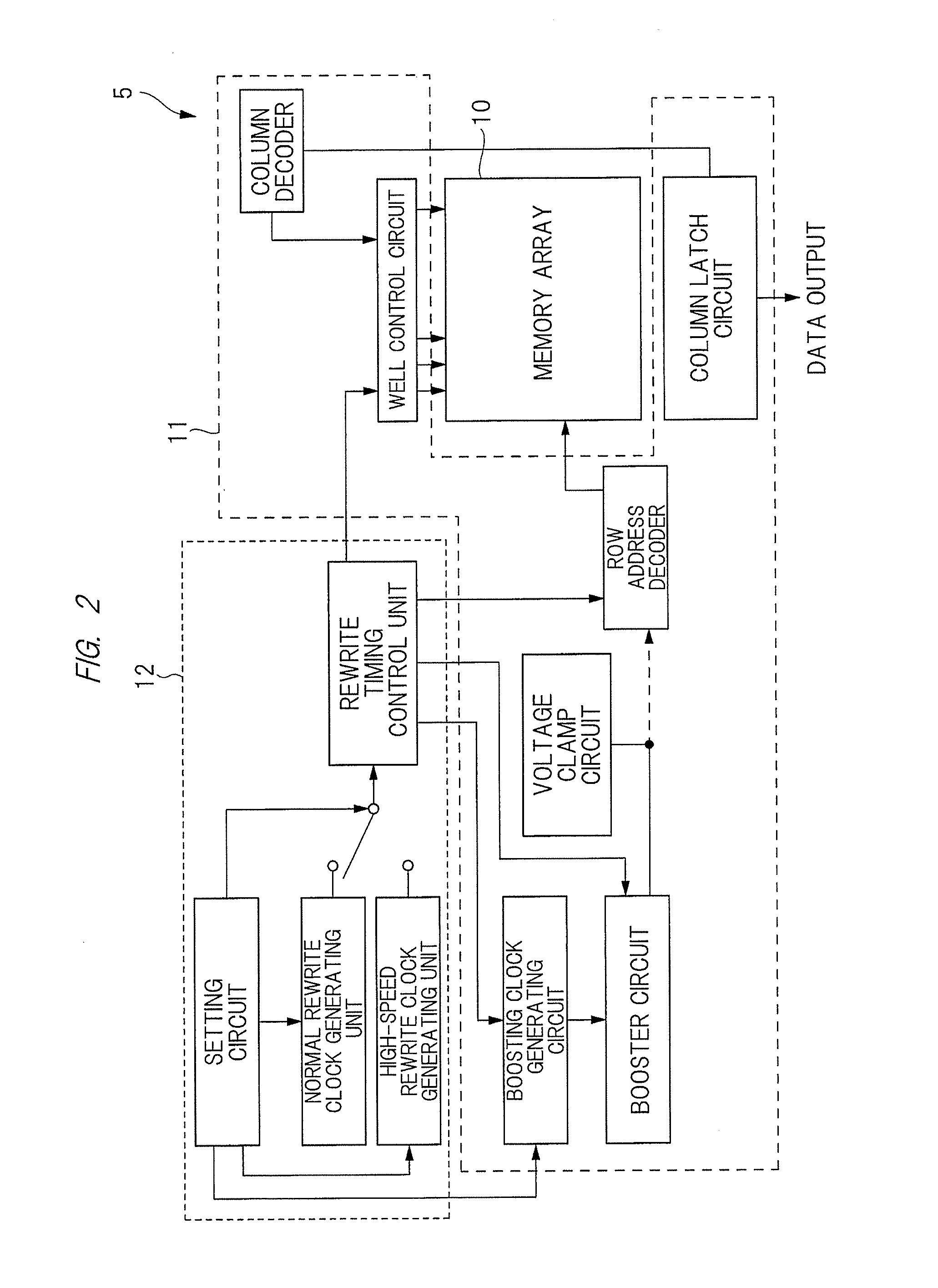
[0043]A technical idea according to the present embodiment is a technical idea that relates to a semiconductor device including, on the same semiconductor chip, a main circuit for achieving a main function of a semiconductor chip and an additional circuit called an add-on circuit which is added to the main circuit, in which the add-on circuit is configured of a rewritable MONOS-type non-volatile memory.

[0044]For example, when a system on chip (SOC) is exemplified, the main circuit is as follows. That is, as the main circuit, a memory circuit such as a dynamic random access memory (DRAM) or a static random access memory (SRAM), a logic circuit such as a central processing unit (CPU) or a micro processing unit (MPU), a mixing circuit of both the memory circuit and the logic circuit, or others, can be exemplified.

[0045]Meanwhile, as the add-on circuit, a memory circuit that stores information of a relatively small volume relating to the main circuit, a fuse to be used for relief of a c...


PUM


Abstract

A performance of a semiconductor device is improved. A film, which is made of silicon, is formed in a resistance element formation region on a semiconductor substrate, and an impurity, which is at least one type of elements selected from a group including a group 14 element and a group 18 element, is ion-implanted into the film, and a film portion which is formed of the film of a portion into which the impurity is ion-implanted is formed. Next, an insulating film with a charge storage portion therein is formed in a memory formation region on the semiconductor substrate, and a conductive film is formed on the insulating film.

Description

CROSS-REFERENCE TO RELATED APPLICATION[0001]The present application claims priority from Japanese Patent Application No. 2015-163136 filed on Aug. 20, 2015, the content of which is hereby incorporated by reference into this application.TECHNICAL FIELD OF THE INVENTION[0002]The present invention relates to a technique of manufacturing a semiconductor device, and relates to effectively applied to, for example, a technique of manufacturing a semiconductor device on which a non-volatile memory is mixedly mounted as an add-on circuit added to a main circuit including a field-effect transistor.BACKGROUND OF THE INVENTION[0003]In a semiconductor device which has a main circuit including a metal insulator semiconductor field effect transistor (MISFET) as a field-effect transistor, an addition circuit (add-on circuit) which is added to a main circuit is formed so as to be separate from the main circuit to achieve a main function of the semiconductor device in some cases. For example, as an e...

Claims


Application Information

Patent Timeline
IPC IPC(8): H01L27/115H01L29/792H01L21/324H01L21/28H01L21/265H01L49/02H01L29/78
CPCH01L27/11573H01L28/20H01L29/792H01L21/324H01L21/28282H01L21/265H01L29/7816H10B43/00H10B43/30H10B43/40H01L27/0629H01L27/088H01L27/0922H01L29/42368H01L29/66659H01L29/7835H01L29/40117H10B43/35H01L29/66833H01L29/66477H01L29/408H01L29/66681H10B43/50H01L21/26513
Inventor YAMAMOTO, YUKIYAMASHITA, TOMOHIRO
Owner RENESAS ELECTRONICS CORP
Why Eureka
Try Eureka