Adaptive Automatic Defect Classification

Active Publication Date: 2017-03-23
KLA TENCOR CORP
View PDF19 Cites 46 Cited by
  • Summary
  • Abstract
  • Description
  • Claims
  • Application Information

AI Technical Summary

Benefits of technology

[0017]FIG. 3 is a flow diagram illustrating one embodiment of steps that may be performed by one or more computer subsystem embodiments described herein for classifying defects with an adaptive automatic defect classifier;
[0018]FIG. 4 is a flow diagram illustrating one embodiment of steps that may be performed by one or more computer subsystem embodiments described herein for determining a data redundancy score;
[0019]FIG. 5 is a flow diagram illustrating one embodiment of steps that may be performed by one or more computer su

Problems solved by technology

For instance, as the dimensions of semiconductor devices decrease, detection of defects of decreasing size has become necessary since even relatively small defects may cause unwanted aberrations in the semiconductor devices.
There are, however, a number of disadvantages to the currently performed methods for defect classifier creation and monitoring.
For example, the classifier creation and monitoring process is cumbersome and cannot provide a relatively fast response to the dynamic defect changes in the fab.
Furthermore, during the training and va

Method used


Image

  • Adaptive Automatic Defect Classification
  • Adaptive Automatic Defect Classification
  • Adaptive Automatic Defect Classification

Examples


Embodiment Construction

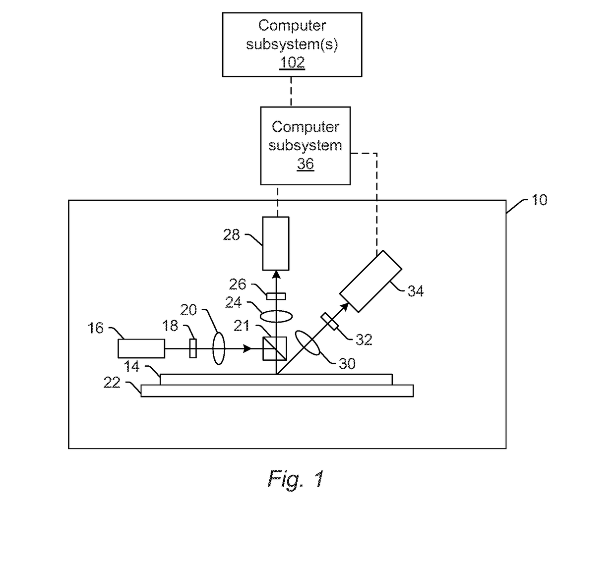
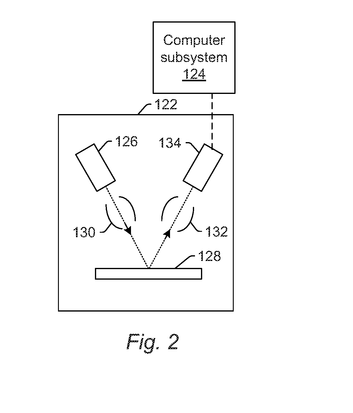
[0023]Turning now to the drawings, it is noted that the figures are not drawn to scale. In particular, the scale of some of the elements of the figures is greatly exaggerated to emphasize characteristics of the elements. It is also noted that the figures are not drawn to the same scale. Elements shown in more than one figure that may be similarly configured have been indicated using the same reference numerals. Unless otherwise noted herein, any of the elements described and shown may include any suitable commercially available elements.

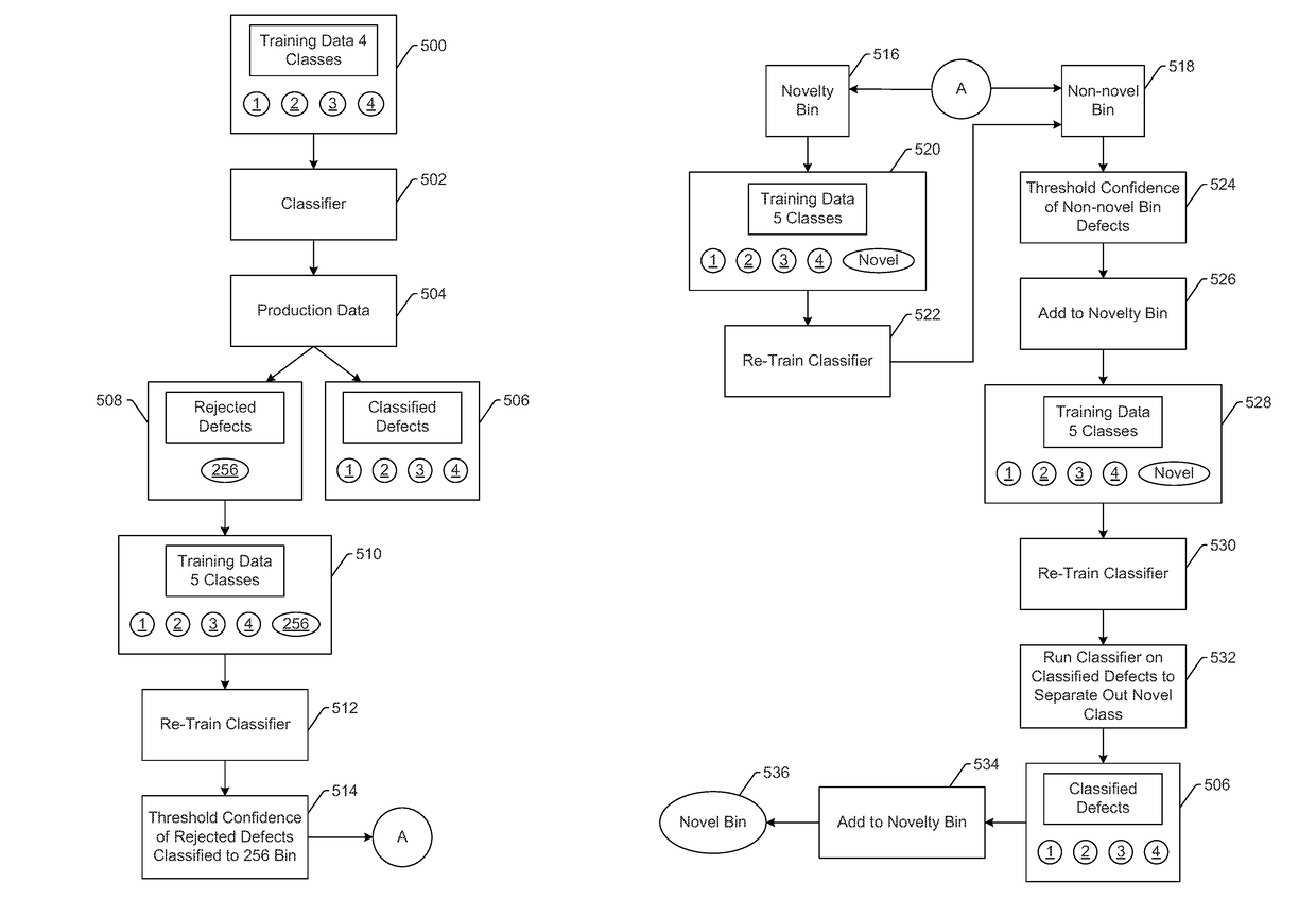
[0024]One embodiment relates to a system configured to classify defects on a specimen with an adaptive automatic defect classifier. The embodiments provide an adaptive strategy to dynamically update and monitor a defect classifier for automatic defect classification (ADC) to adapt to the dynamic environment of a semiconductor fabrication process. The embodiments also provide a data redundancy score (DRS) generated using the adaptive strategy, where D...


PUM


Abstract

Methods and systems for classifying defects detected on a specimen with an adaptive automatic defect classifier are provided. One method includes creating a defect classifier based on classifications received from a user for different groups of defects in first lot results and a training set of defects that includes all the defects in the first lot results. The first and additional lot results are combined to create cumulative lot results. Defects in the cumulative lot results are classified with the created defect classifier. If any of the defects are classified with a confidence below a threshold, the defect classifier is modified based on a modified training set that includes the low confidence classified defects and classifications for these defects received from a user. The modified defect classifier is then used to classify defects in additional cumulative lot results.

Description

BACKGROUND OF THE INVENTION[0001]1. Field of the Invention[0002]This invention generally relates to methods and systems for classifying defects on a specimen with an adaptive automatic defect classifier.[0003]2. Description of the Related Art[0004]The following description and examples are not admitted to be prior art by virtue of their inclusion in this section.[0005]Fabricating semiconductor devices such as logic and memory devices typically includes processing a substrate such as a semiconductor wafer using a large number of semiconductor fabrication processes to form various features and multiple levels of the semiconductor devices. For example, lithography is a semiconductor fabrication process that involves transferring a pattern from a reticle to a resist arranged on a semiconductor wafer. Additional examples of semiconductor fabrication processes include, but are not limited to, chemical-mechanical polishing, etch, deposition, and ion implantation. Multiple semiconductor dev...

Claims


Application Information

Patent Timeline
IPC IPC(8): G01N21/95G06N99/00G06N20/10G06N20/20
CPCG01N21/9501G01N2201/12G01N2201/06113G06N99/005G01N21/8851G01N2021/8854G01N2021/8883H01L22/12H01L22/20G06N20/00G06N20/20G06N20/10H01L22/24H01L22/34
Inventor HE, LIPLIHAL, MARTINYING, HUAJUNBHATIA, ANADIDANDIANA, AMITOZ SINGHRAMINI, RAMAKANTH
Owner KLA TENCOR CORP
Why Eureka
Try Eureka