Stacked Nanowires

a nanowire and stacked technology, applied in the direction of basic electric elements, electrical equipment, semiconductor devices, etc., can solve the problems of parasitic ge nanowires (or sige nanowires with high ge content) and achieve the effect of reducing the formation of parasitic ge nanowires

Active Publication Date: 2017-04-13
IBM CORP
View PDF0 Cites 89 Cited by
  • Summary
  • Abstract
  • Description
  • Claims
  • Application Information

AI Technical Summary

Benefits of technology

[0005]In another aspect of the invention, a method of forming a field effect transistor (FET) device is provided. The method includes the steps of: forming a stack of alternating Si and SiGe layers on a wafer; patterning fins in the stack; selectively thinning the SiGe layers in the fins such that the Si and SiGe layers give the fins an hourglass shape; burying the fins in an oxide material; annealing the fins under conditions sufficient to diffuse Ge from the SiGe layers in the fins to the Si layers in the fins to form one or more stacks of SiGe nanowires; releasing the SiGe nanowires from the oxide material in a channel region of the FET device; and forming a gate surrounding a portion of each of the SiGe nanowires in the channel region of the FET device, wherein portions of the SiGe nanowires extending out from the gate serve as source and drain regions of the FET device.

Problems solved by technology

However, a practical problem is found that when condensation is performed on Si / SiGe stacks, parasitic Ge nanowires (or SiGe nanowires with high Ge content) are formed.

Method used


Image

  • Stacked Nanowires
  • Stacked Nanowires
  • Stacked Nanowires

Examples


Embodiment Construction

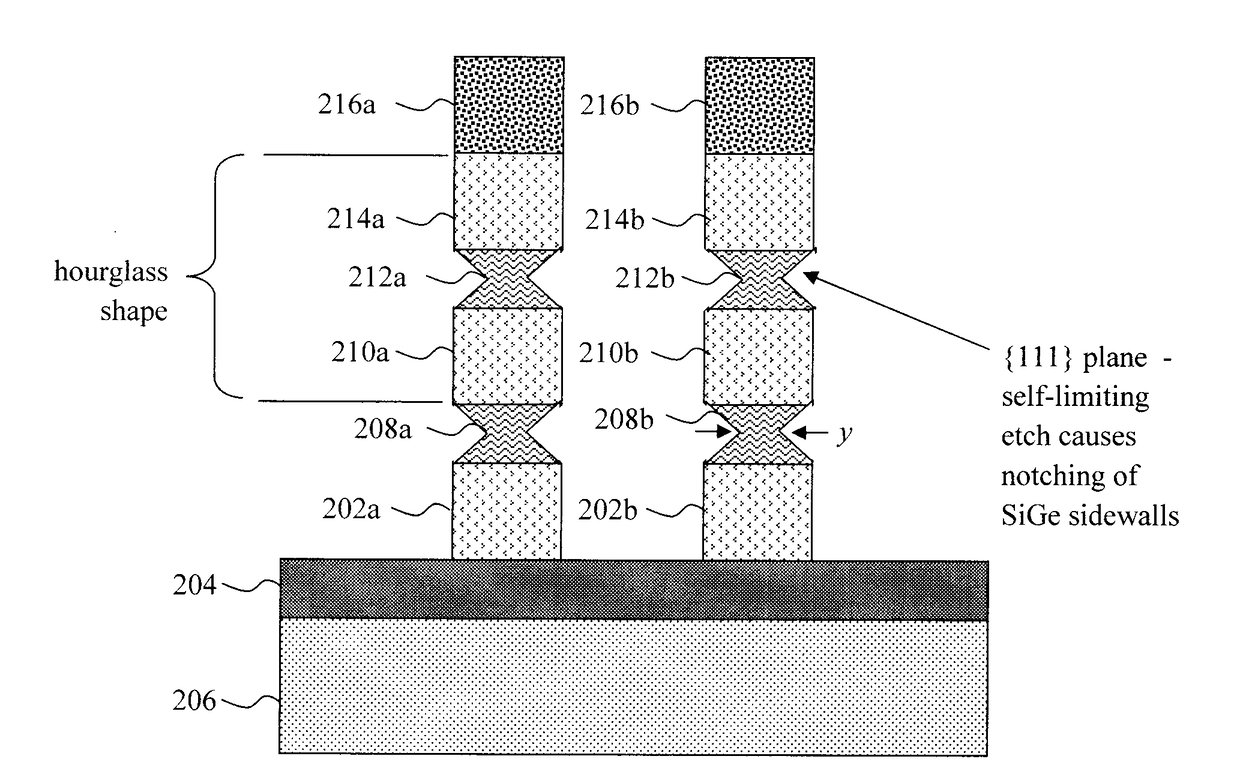
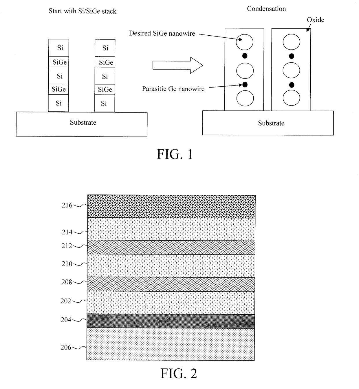
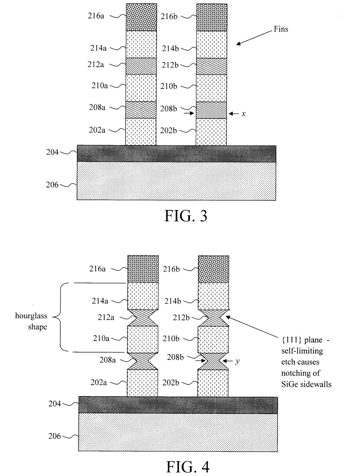
[0032]As provided above, a condensation process is often used to form SiGe nanowires. Such a process leverages the preferential oxidation of silicon (Si) over germanium (Ge), whereby the expelled Ge can be used to form SiGe nanowires. Take for example a process wherein a fin is provided containing alternating layers of SiGe and Si. A condensation process can be employed to diffuse the Ge from the SiGe layers into the Si layers, forming SiGe nanowires. However, a problem with this process exists because some of the Ge is driven to the SiGe layer core, forming parasitic Ge nanowires in between the SiGe nanowires. See, for example, FIG. 1.

[0033]As shown in FIG. 1, beginning with a fin stack alternating Si and SiGe layers, a condensation process can be used to diffuse Ge from the SiGe layers into the Si layers, forming the desired SiGe nanowires. However, some of the Ge will get driven to the SiGe layer core, undesirably forming parasitic Ge nanowires (or SiGe nanowires with high Ge con...


PUM

PropertyMeasurementUnit
widthaaaaaaaaaa
widthaaaaaaaaaa
temperatureaaaaaaaaaa

Abstract

Techniques for producing stacked SiGe nanowires using a condensation process without parasitic Ge nanowires as an undesired by-product. In one aspect, a method of forming SiGe nanowires includes the steps of: forming a stack of alternating Si and SiGe layers on a wafer; patterning fins in the stack; selectively thinning the SiGe layers in the fins such that the Si and SiGe layers give the fins an hourglass shape; burying the fins in an oxide material; and annealing the fins under conditions sufficient to diffuse Ge from the SiGe layers in the fins to the Si layers in the fins to form the SiGe nanowires. A FET device and method for formation thereof are also provided.

Description

FIELD OF THE INVENTION[0001]The present invention relates to techniques for producing stacked nanowires, and more particularly, to producing stacked silicon germanium (SiGe) nanowires using a condensation process without parasitic germanium (Ge) nanowires as an undesired by-product.BACKGROUND OF THE INVENTION[0002]Silicon germanium (SiGe) nanowires are desired for p-channel field effect transistor (PFET) devices. A common technique for forming SiGe nanowires is a so-called ‘condensation’ process, wherein preferential oxidation of silicon (Si) and condensing Ge is used to form SiGe nanowires. However, a practical problem is found that when condensation is performed on Si / SiGe stacks, parasitic Ge nanowires (or SiGe nanowires with high Ge content) are formed.[0003]Therefore, techniques for making SiGe nanowire channeled PFETs without the creation of parasitic Ge nanowires would be desirable.SUMMARY OF THE INVENTION[0004]The present invention provides techniques for producing stacked s...

Claims


Application Information

Patent Timeline
Patent Type & Authority Applications(United States)
IPC IPC(8): H01L29/06H01L29/78H01L29/417H01L21/3105H01L21/02H01L21/306H01L21/324H01L29/66H01L29/423
CPCH01L29/0676H01L29/66545H01L29/66795H01L29/66553H01L29/785H01L29/41791H01L2029/7858H01L21/02603H01L21/02532H01L21/30608H01L21/324H01L21/3105H01L29/42392H01L29/66439H01L29/775H01L29/78696
Inventor BI, ZHENXINGCHENG, KANGGUOLI, JUNTAOMIAO, XIN
Owner IBM CORP
Why Eureka
Try Eureka