

Power Driven Optimization For Flash Memory
a flash memory and power-driven technology, applied in the direction of static storage, electrical appliances, instruments, etc., can solve the problems of increasing the power consumption affecting the performance or state of the memory array, and unduly shortening the lifespan of the memory array
- Summary
- Abstract
- Description
- Claims
- Application Information
AI Technical Summary
Benefits of technology
Problems solved by technology
Method used
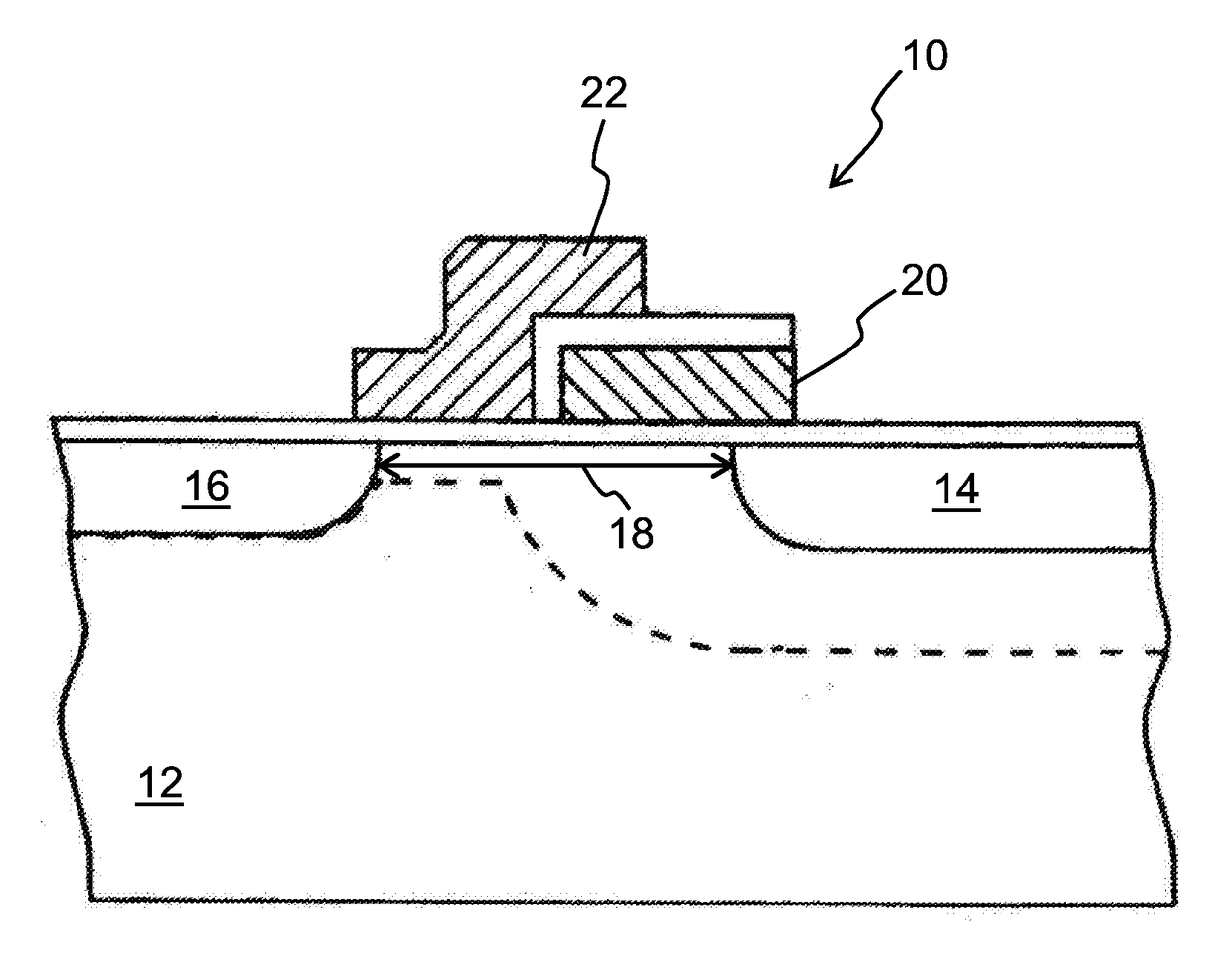
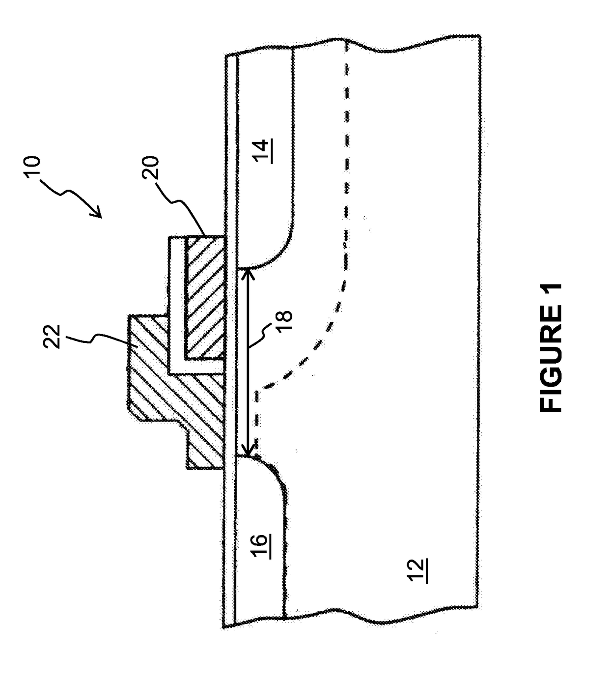
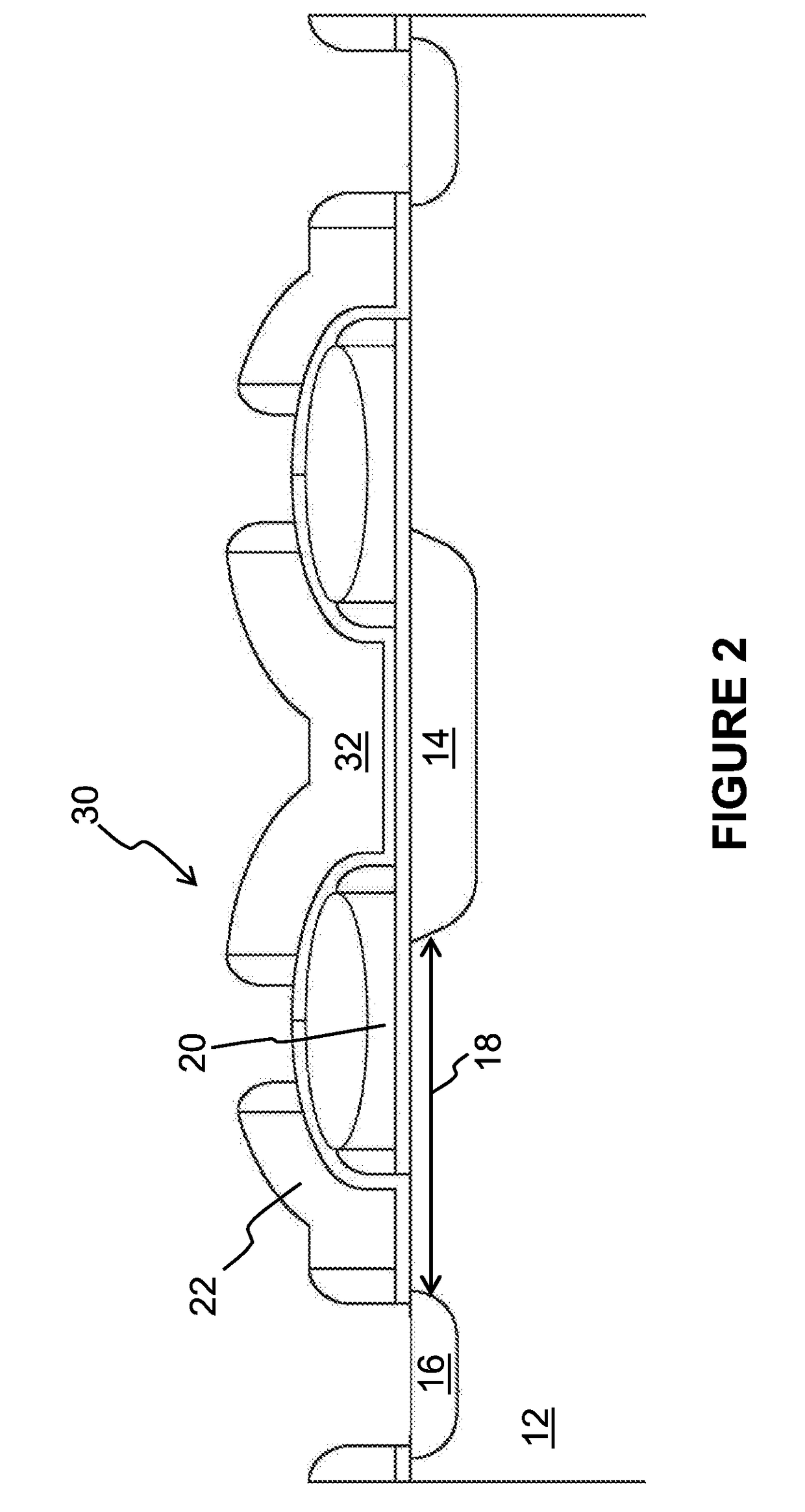
Image

Examples
example 1
[0027]Standard Erase Operation=one 11 volt pulse of 10 ms in duration.
[0028]Lower Energy Margin Erase Operation:[0029](a) shorter duration: one 11 volt pulse of 5 ms in duration, or[0030](b) lower voltage pulse: one 10 volt pulse of 10 ms in duration, or[0031](c) a combination of both (a) and (b) above.
example 2
[0032]Standard Erase Operation=4 pulses each of 1 ms, 11 volts
[0033]Lower Energy Margin Erase Operation[0034](a) fewer pulses: 2 pulses each of 1 ms, 11 volts, or[0035](b) lower voltage pulses: 4 pulses each of 1 ms, 10 volts, or[0036](c) shorter pulses: 4 pulses each of 0.5 ms, 11 volts, or[0037](d) any combination of (a)-(c) above.
example 3
[0038]Standard Program Operation=one 8 volt pulse of 10 μs in duration
[0039]Lower Energy Margin Program Operation[0040](a) shorter duration=one 8 volt pulse of 5 μs in duration, or[0041](b) lower voltage pulse: one 6 volt pulse of 10 μs in duration, or[0042](c) a combination of both (a) and (b) above.
PUM
 Abstract
Description
Claims
Application Information