

Optical approximate correction method and its photomask pattern
An optical approximation correction and photomask technology, which is applied in optics, microlithography exposure equipment, and originals for photomechanical processing, etc., can solve the problems of reducing device yield and improve yield, focus depth and energy The effect of increased margin, depth of focus, and increased energy margin
- Summary
- Abstract
- Description
- Claims
- Application Information
AI Technical Summary
Problems solved by technology
Method used
Image

Examples
Embodiment Construction
[0064] The specific embodiments of the present invention will be described in detail below in conjunction with the accompanying drawings. The drawings are not intentionally drawn to scale, and therefore are not intended to limit the scope of protection of the claims of the present invention.
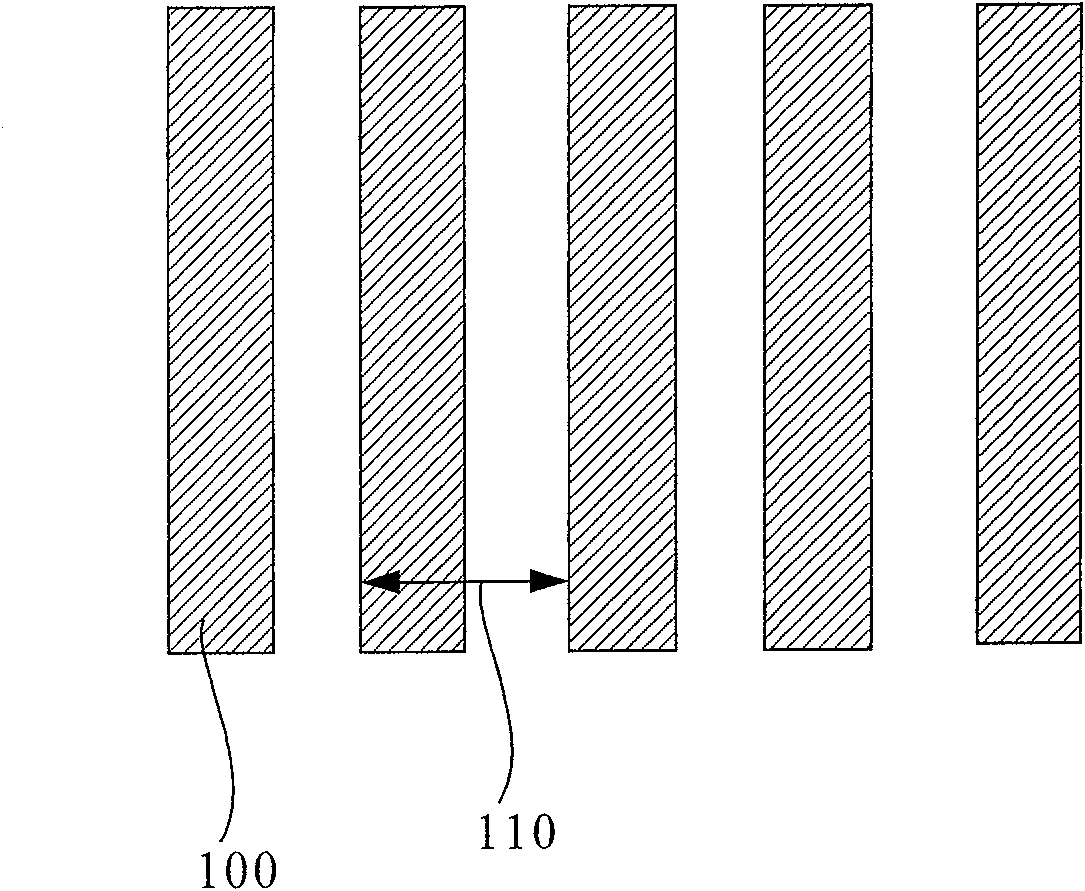
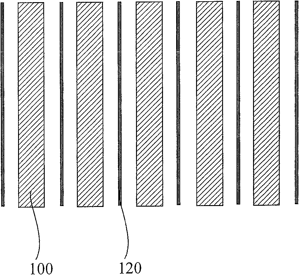
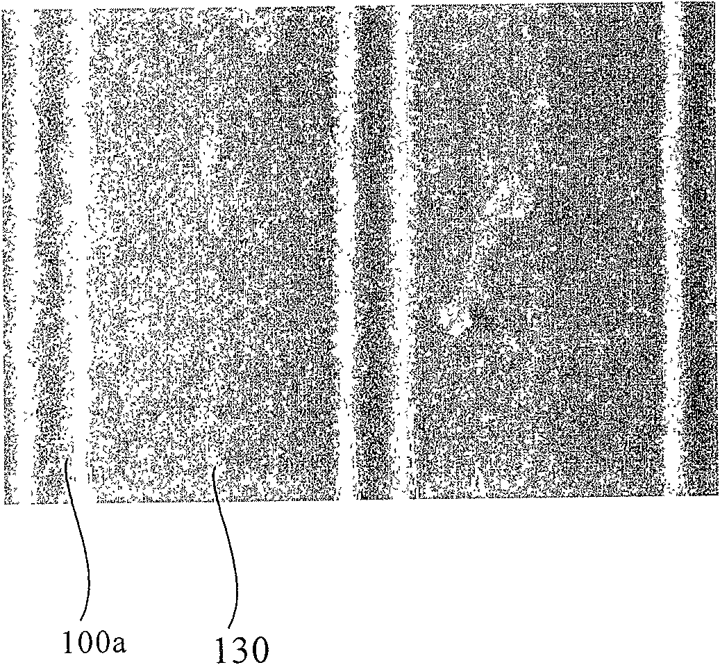
[0065] Optical interference and diffraction effects are bottlenecks in the reduction of critical dimensions of semiconductors. In general, for a particular wavelength, the resolution is that wavelength itself. For example, for a 248nm ultraviolet light source, its resolvable scale is only 248nm. With the help of the optimization of the optical system parameters, the resolution of the entire exposure machine can be greatly improved. For example, the off-axis illumination method is used to compress the first-order diffraction angle of the light passing through the mask, and the phase shift technology is used to change the phase of the pattern after the light passes through the mask. And ...
PUM
 Abstract
Description
Claims
Application Information