Laser array display

a laser array and display technology, applied in the field of displays, can solve the problem of typically smaller angular dispersion of lasers than is desired, and achieve the effect of increasing the light-output efficiency and resolution of micro-led lasers, reducing substrate and assembly costs

Active Publication Date: 2017-05-11
X DISPLAY CO TECH LTD
View PDF13 Cites 77 Cited by
  • Summary
  • Abstract
  • Description
  • Claims
  • Application Information

AI Technical Summary

Benefits of technology

[0016]The micro-light-emitting diode lasers can be made using crystalline semiconductors in a semiconductor wafer and then micro-transfer printed to a display substrate, for example a glass substrate, thus increa

Problems solved by technology

However, the angular dispersion of a laser is t

Method used


Image

  • Laser array display
  • Laser array display
  • Laser array display

Examples


Embodiment Construction

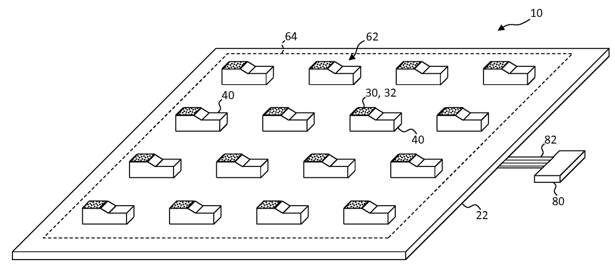
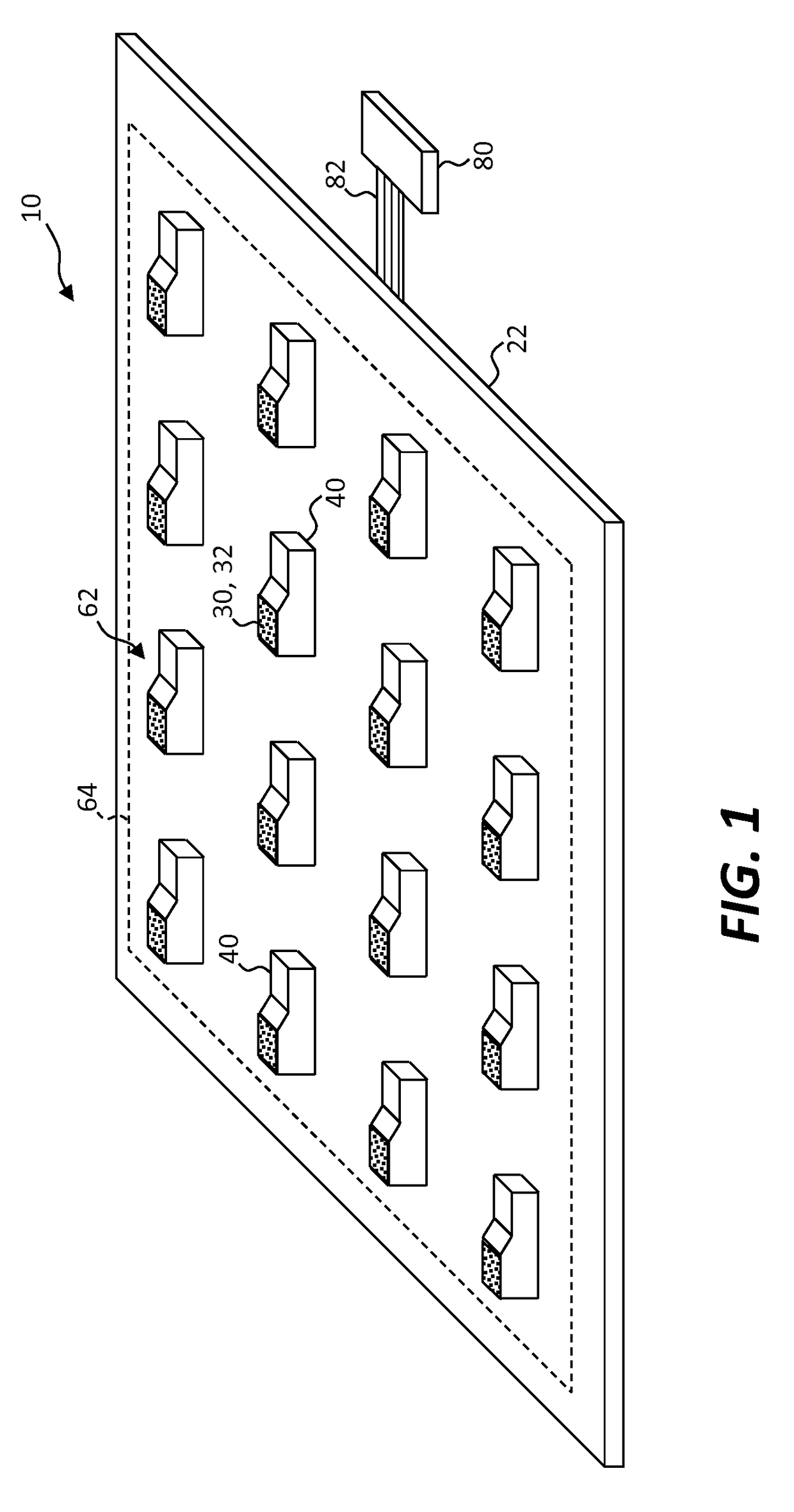
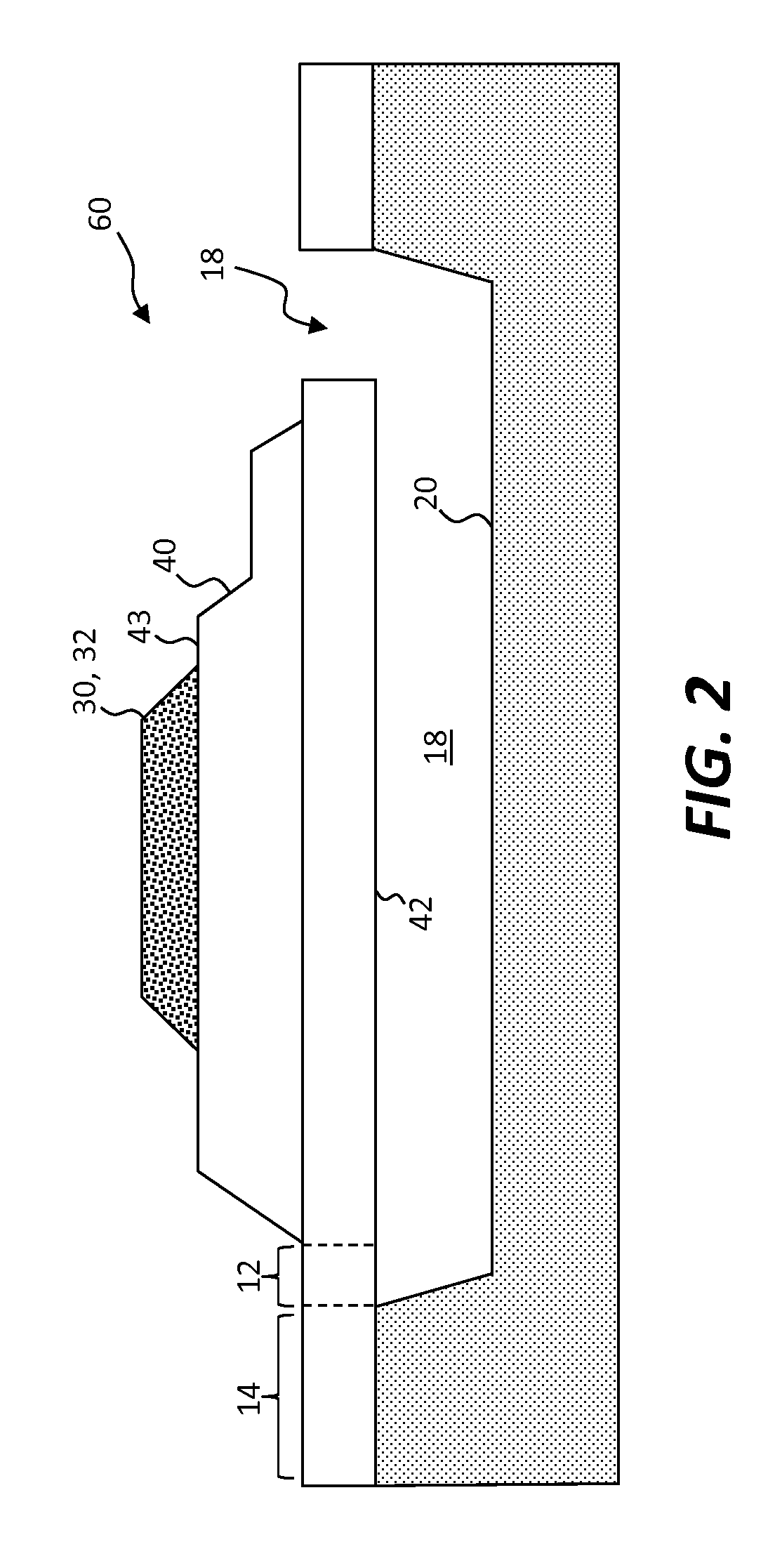
[0028]Referring to FIG. 1, an embodiment of the present invention provides a micro-LED laser display 10 comprising a display substrate 22 for displaying an image and an array 64 of display pixels 62. Each display pixel 62 has one or more micro-LED lasers 40 disposed on the display substrate 22 that emit light within an emission angle to form an image pixel. In the example shown in FIG. 1, each display pixel 62 includes a single micro-LED laser 40. In alternative examples, each display pixel 62 includes more than one (e.g., three) micro-LED lasers 40. One or more light spreaders 30 are located in correspondence to one or more of the micro-LED lasers 40 to increase the emission angle of light emitted by each micro-LED laser 40. A controller 80 individually controls the micro-LED lasers 40, for example with electrical signals transmitted to the micro-LED lasers 40 through a bus 82 connected to the controller 80.

[0029]The light spreaders 30 can have various structures and include variou...


PUM


Abstract

A micro-LED laser display having an array of display pixels includes a display substrate for displaying an image and an array of display pixels. Each display pixel has one or more micro-LED lasers disposed on the display substrate. Each micro-LED laser emits light within an emission angle. One or more light spreaders for increasing the emission angle of light emitted by each micro-LED laser are disposed in relation to the light spreaders and a controller individually controls the micro-LED lasers.

Description

CROSS REFERENCE TO RELATED APPLICATIONS[0001]This application is related to commonly assigned U.S. patent application Ser. No. 14 / 930,363 filed Nov. 2, 2015, entitled Display with Color Conversion, U.S. patent application Ser. No. 14 / 788,632 filed Jun. 30, 2015, entitled Inorganic Light-Emitting Diode with Encapsulating Reflector, U.S. patent application Ser. No. 14 / 743,967 filed Jun. 18, 2015, entitled Micro-Assembled LED Displays and Lighting Elements, U.S. patent application Ser. No. 14 / 743,975 filed Jun. 18, 2015, entitled Micro Assembled LED Displays and Lighting Elements, U.S. patent application Ser. No. 14 / 743,984 filed Jun. 18, 2015, entitled Systems and Methods for Preparing GaN and Related Materials for Micro Assembly, U.S. patent application Ser. No. 14 / 743,988 filed Jun. 18, 2015, entitled Systems and Methods for Controlling Release of Transferable Semiconductor Structures, and U.S. patent application Ser. No. 14 / 807,311 filed Jul. 23, 2015, entitled Printable Inorganic ...

Claims


Application Information

Patent Timeline
IPC IPC(8): H01S5/00G02F1/1335G02B27/48G02B5/00G02B5/02G02B3/00
CPCH01S5/005G02B5/0242G02B3/0006G02F2001/133607G02B5/003G02F1/133606G02B27/48G09F9/33H01L25/0753H01S5/423G02F1/133603H01L33/20G02F1/133607H01L2224/24
Inventor COK, RONALD S.
Owner X DISPLAY CO TECH LTD
Why Eureka
Try Eureka