Pixel electrode and liquid crystal display panel

Active Publication Date: 2017-05-25
TCL CHINA STAR OPTOELECTRONICS TECH CO LTD
View PDF1 Cites 5 Cited by
  • Summary
  • Abstract
  • Description
  • Claims
  • Application Information

AI Technical Summary

Benefits of technology

[0060]The benefits of the present invention are: in the liquid crystal display panel of the present invention, by locating the main parts to be elbow bend zigzag structures to make the liquid crystal molecules of the main electrode position be aligned along a tilt 45 degrees direction as possible, the active area is enlarged to solve the issue that the penetration rate is low because the liquid crystal molecules at the structure of the (cross) keel of pozidriv pixel electrode fall d

Problems solved by technology

However, because the VA liquid crystal display utilizes vertical twist liquid crystals and the birefraction differe

Method used


Image

  • Pixel electrode and liquid crystal display panel
  • Pixel electrode and liquid crystal display panel
  • Pixel electrode and liquid crystal display panel

Examples


first embodiment

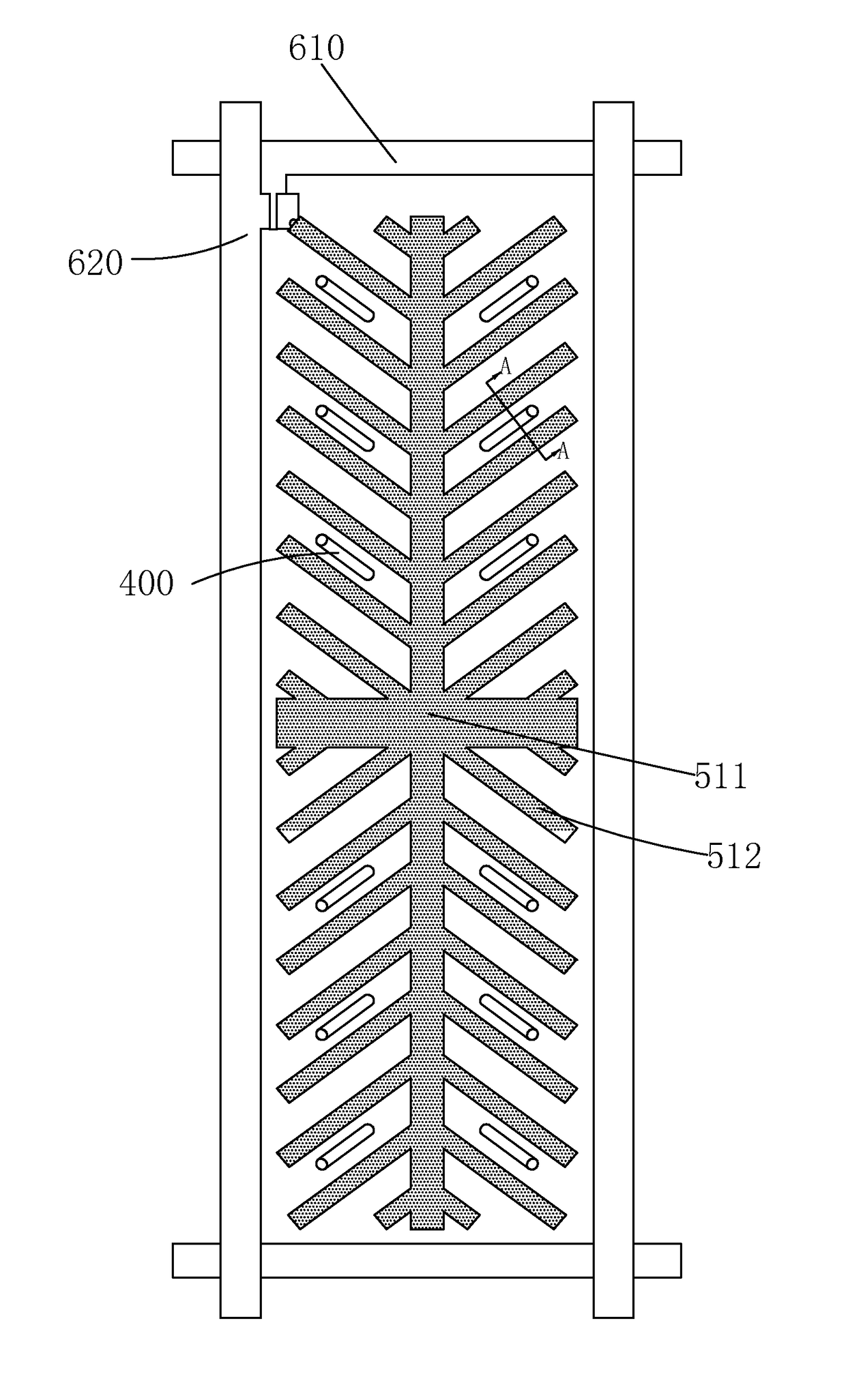
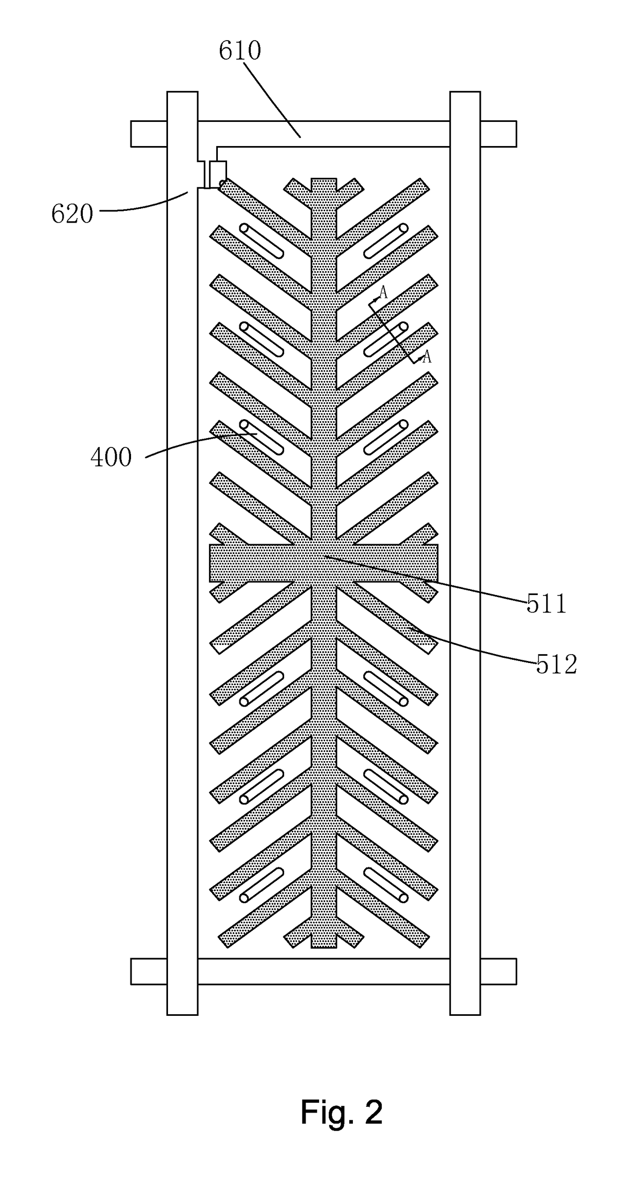
[0084]Specifically, in the first embodiment, and in the first region, one sides of the first electrode sections 11, third electrode sections 21 close to the first region are orthogonally connected with one first branch electrode 81, respectively, and the first branch electrode 81 is connected with the first bending part 71 or the second bending part 72;

[0085]in the second region, one sides of the second electrode sections 12, fourth electrode sections 22 close to the second region are orthogonally connected with one second branch electrode 82, respectively, and the second branch electrode 82 is connected with the first bending part 71 or the second bending part 72;

[0086]in the third region, one sides of the first electrode sections 11, third electrode sections 21 close to the third region are orthogonally connected with one third branch electrode 83, respectively, and the third branch electrode 83 is connected with the first bending part 71 or the second bending part 72;

[0087]in the...

second embodiment

[0114]Please refer from FIG. 8 to FIG. 9. The pixel electrode 52 at one side of the lower substrate 20 can utilize any one structure of the first and second embodiment of the aforesaid pixel electrode (as shown in FIG. 5 and FIG. 6). The repeated description is omitted here.

[0115]As the pixel electrode of the present invention is applied in a liquid crystal display panel, the plurality of first, second, third and fourth branch electrodes 81, 82, 83, 84 respectively correspond to four areas of one sub pixel area. As applying voltage to the liquid crystal display panel, because the main part of the pixel electrode of the present invention is not the structure of the (cross) keel but two crossing elbow bend zigzag structures, the active area is enlarged to reduce the issue that the liquid crystal molecules fall down toward the improper directions and to make the liquid crystal molecules in the region corresponding to the original structure of the (cross) keel to be aligned along the di...


PUM


Abstract

The present invention provides a pixel electrode and a liquid crystal display panel. In the liquid crystal display panel of the present invention, by locating the main parts to be elbow bend zigzag structures to make the liquid crystal molecules of the main electrode position be aligned along a tilt 45 degrees direction as possible, the active area is enlarged to solve the issue that the penetration rate is low because the liquid crystal molecules at the structure of the (cross) keel of pozidriv pixel electrode fall down toward the improper directions, to raise the penetration rate for reducing the demand to the backlight brightness of the liquid crystal display panel and lowering the cost and the usage power consumption. In the liquid crystal display panel of the present invention, of which the main parts of the pixel electrode utilizes the elbow bend zigzag structures, the penetration rate is higher, and the demand to the backlight brightness is lower, and the usage power consumption is lower.

Description

FIELD OF THE INVENTION[0001]The present invention relates to a display technology field, and more particularly to a pixel electrode and a liquid crystal display panel.BACKGROUND OF THE INVENTION[0002]In recent years, the Thin Film Transistor-LCD (TFT-LCD) has been rapidly developed and applied widely. For the TFT-LCD in the mainstream market, three types, which respectively are Twisted Nematic (TN), Super Twisted Nematic (STN), In-Plane Switching (IPS) and Vertical Alignment (VA) can be illustrated. The VA liquid crystal display possesses extremely high contrast than the liquid crystal displays of other types, which can reach up to 4000-8000 in general. It has very wide application in large scale display, such as television or etc.[0003]The reason why the VA liquid crystal display possesses extremely high contrast is that the liquid crystal molecules are vertically aligned to the substrate surface, and no phase difference exists, and light leakage is very small, and the dark state b...

Claims


Application Information

Patent Timeline
IPC IPC(8): G02F1/1343G02F1/1362G02F1/1368
CPCG02F1/134309G02F1/13439G02F2201/121G02F1/136286G02F2201/123G02F1/1368G02F1/133707
Inventor ZHONG, XINHUI
Owner TCL CHINA STAR OPTOELECTRONICS TECH CO LTD
Why Eureka
Try Eureka