Controlled doping from low to high levels in wide bandgap semiconductors

a wide bandgap semiconductor and controlled doping technology, applied in semiconductor devices, semiconductor lasers, semiconductor devices, etc., can solve the problem that the fermi level is not a free parameter that is easily modified, and achieve the effect of improving the doping capability, increasing the efficiency and operational range of ultraviolet light, and efficient use and transmission of electrical energy

Inactive Publication Date: 2017-06-01
NORTH CAROLINA STATE UNIV
View PDF7 Cites 0 Cited by
  • Summary
  • Abstract
  • Description
  • Claims
  • Application Information

AI Technical Summary

Benefits of technology

[0006]Many applications such as optoelectronics and power electronics rely on the functionality of wide bandgap materials. But to reach their full potential, it is necessary to realize point defect control in order to enhance the doping capabilities. Examples of the possibilities of the proposed enabling technology are increasing the efficiency and operational range of ultraviolet (UV) light emitting diodes (LEDs), deep ultraviolet (DUV) laser diodes, power rectifiers, as well as switches. This research will directly lead to materials that will be used for applications that deal with the preservation and extension of natural resources by allowing for: (1) the efficient use and transmission of electrical energy, (2) the availability of clean potable water through disinfection by the use of UV LEDs, and (3) the detection of pollutants and other effluents.

Problems solved by technology

This is a fundamental problem with wide bandgap materials.
It has been traditionally understood that the Fermi level is not a free parameter easily modified during an experiment and is only controlled by doping.

Method used


Image

  • Controlled doping from low to high levels in wide bandgap semiconductors
  • Controlled doping from low to high levels in wide bandgap semiconductors
  • Controlled doping from low to high levels in wide bandgap semiconductors

Examples


Embodiment Construction

[0033]The present disclosure will now be described more fully hereinafter with reference to example implementations thereof. These example implementations are described so that this disclosure will be thorough and complete, and will fully convey the scope of the disclosure to those skilled in the art. Indeed, the disclosure may be embodied in many different forms and should not be construed as limited to the implementations set forth herein; rather, these implementations are provided so that this disclosure will satisfy applicable legal requirements. As used in the specification and the appended claims, the singular forms “a,”“an,”“the” and the like include plural referents unless the context clearly dictates otherwise. Also, for example, reference may be made herein to quantitative measures, values, relationships or the like (e.g., planar, coplanar, perpendicular). Unless otherwise stated, any one or more if not all of these may be absolute or approximate to account for acceptable ...


PUM


Abstract

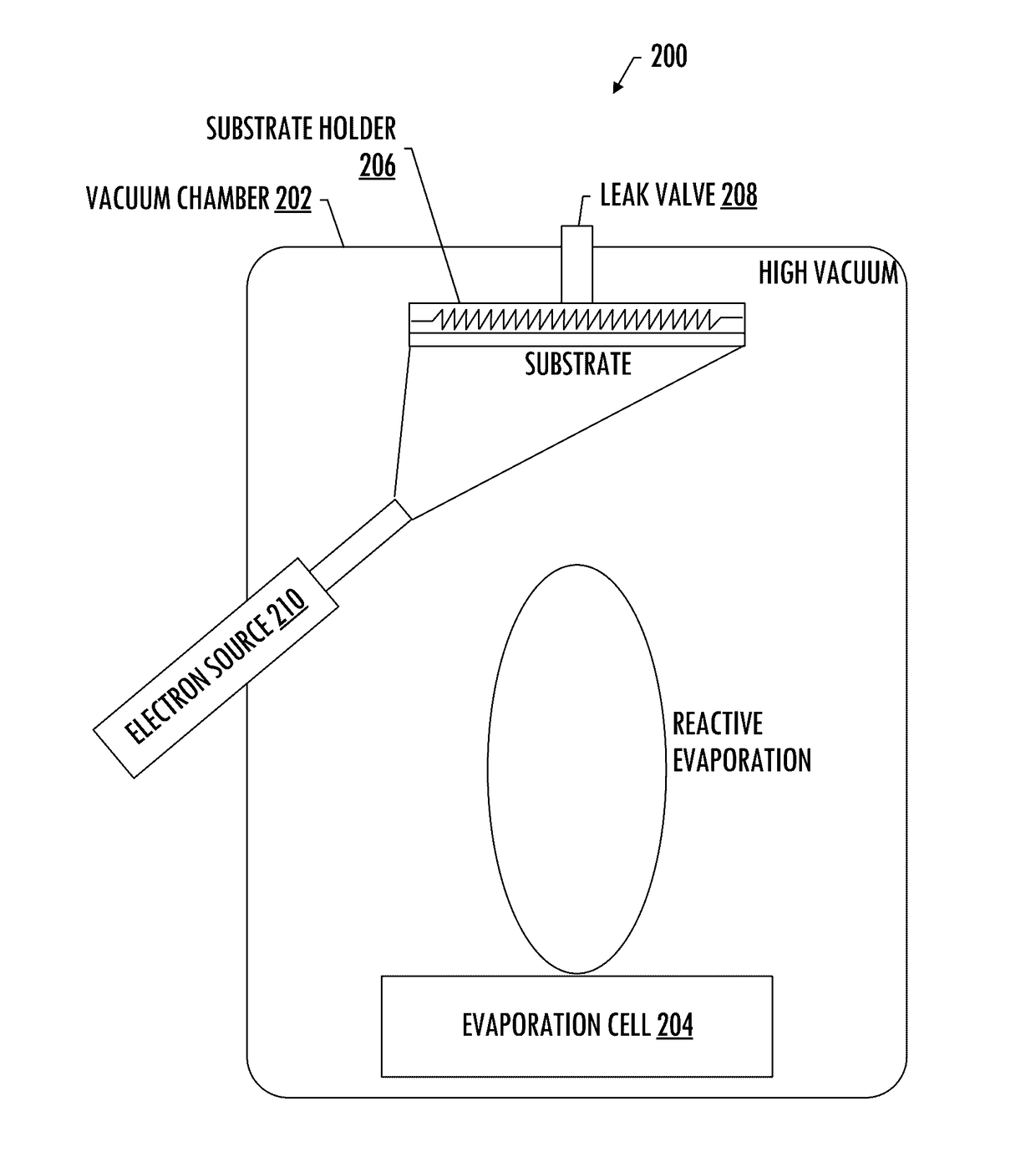
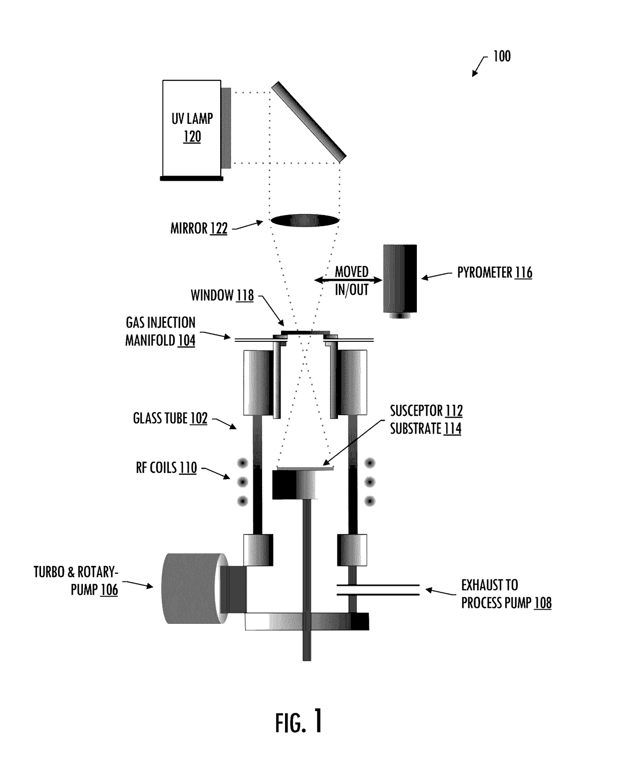
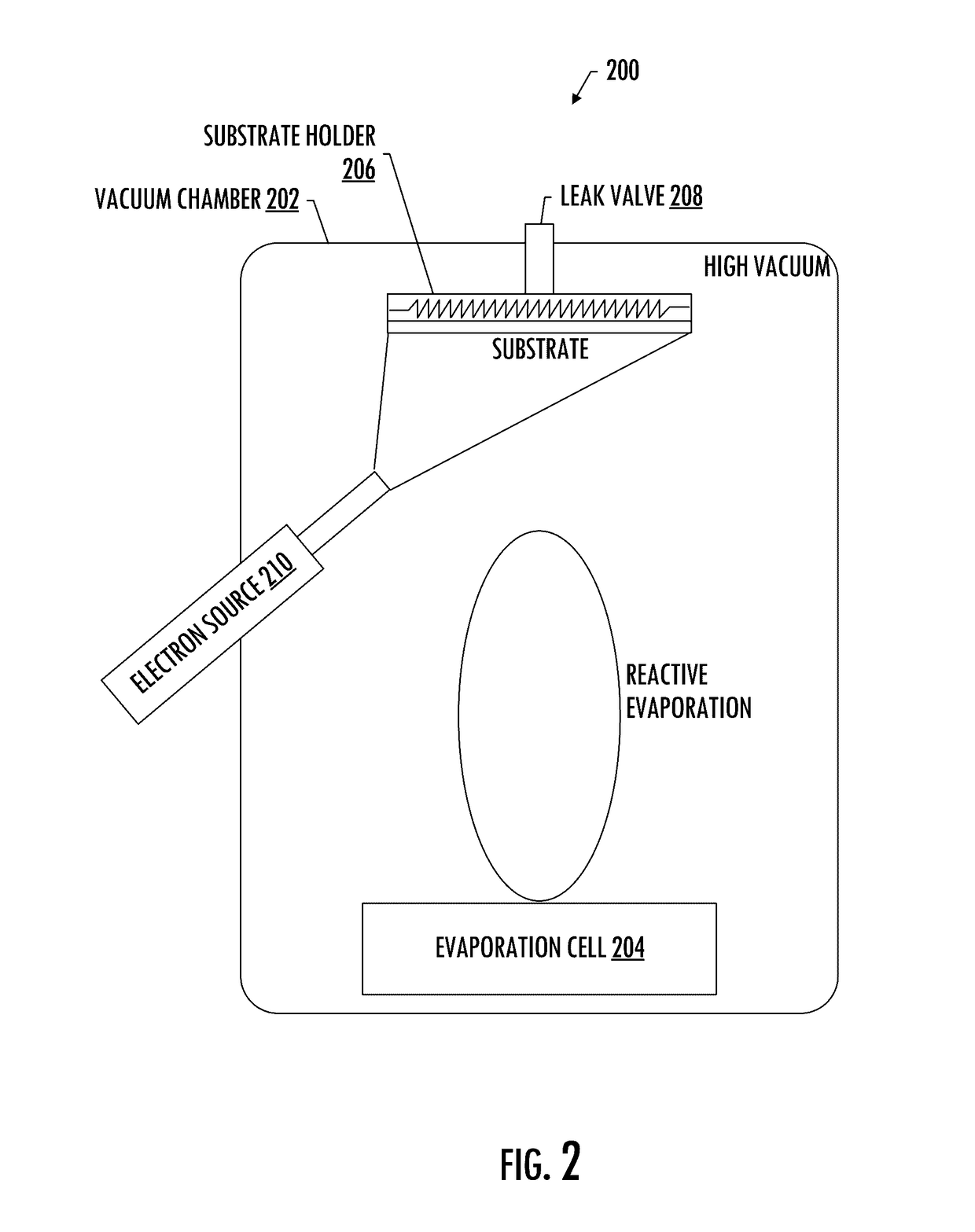
The energy of formation of a point defect in a compound semiconductor is a function of the process conditions and the Fermi energy (the energy of the charge carriers). In wide bandgap semiconductors or insulators, the contribution of this energy to the formation energy of charged point defects is significant. For doping for n- or p-type conductivity, the larger the energy gap, the higher the concentration of compensating point defects that is at equilibrium with the system. This is a fundamental problem with wide bandgap materials that will be directly addressed with these capabilities. In this approach, minority carrier injection is used to modify the quasi-Fermi level to control the formation energy of the point defects. Increasing the formation energy of unwanted point defect through an external excitation that leads to excess minority carriers during the growth of the semiconductor device structure leads to a reduction in compensating point defects.

Description

CROSS-REFERENCE TO RELATED APPLICATION(S)[0001]The present application claims priority to U.S. Provisional Patent Application No. 62 / 261,110, entitled: Controlled Doping from Low to High Levels in Wide Bandgap Semiconductors, filed on Nov. 30, 2015, the content of which is incorporated herein by reference.BACKGROUND[0002]Charged point defects in compound semiconductors strongly determine electronic and optical properties. The energy of formation of a point defect is a function of the process conditions and the Fermi energy. In wide bandgap semiconductors or insulators, the contribution of the Fermi energy to the formation energy of charged point defects is significant. For the practical case of doping for n- or p-type conductivity, the larger the energy gap, the higher the concentration of compensating point defects that is at equilibrium with the system. This is a fundamental problem with wide bandgap materials.[0003]Therefore, it may be desirable to have a method and apparatus tha...

Claims


Application Information

Patent Timeline
Patent Type & Authority Applications(United States)
IPC IPC(8): H01L29/20H01L33/32H01L21/263H01L33/00H01L21/268H01L21/67H01L29/36H01S5/30
CPCH01L29/2003H01L29/36H01L33/32H01L21/263H01L33/0075H01L21/2686H01L21/67115H01S5/3013H01L21/0254H01L21/02576H01L21/02579H01L21/0262H01S5/32341H01S2304/04
Inventor COLLAZO, RAMON R.SITAR, ZLATKOTWEEDIE, JAMES
Owner NORTH CAROLINA STATE UNIV
Why Eureka
Try Eureka