Photonic crystal superprism with ultra-high resolution and design method therefor

a photonic crystal and superprism technology, applied in the field of photoelectron and optical communication, can solve the problems of not conducive to the application of the device in the integrated optical path, and achieve the effects of wide application range, good integrality, and convenient auto-collimation area

Active Publication Date: 2017-06-15
SHANGHAI INST OF MICROSYSTEM & INFORMATION TECH CHINESE ACAD OF SCI +1
View PDF0 Cites 0 Cited by
  • Summary
  • Abstract
  • Description
  • Claims
  • Application Information

AI Technical Summary

Benefits of technology

[0026]As described above, the ultrahigh-resolution photonic-crystal superprism of the present invention and the method for designing the same have the following beneficial effects: the present invention optimizes the structure parameter of the photonic crystal to facilitate the auto-collimation area and the low group velocity area in the equifrequency graph of the photonic crystal to be overlapped as much as possible, defines the overlapping area as a work area, appropriately rotates the photonic crystal to intersect the equal incidence-angle line with the work area, selects the appropriate incidence angle, and facilitates the incidence angle to be a right angle as much as possible to conveniently design the optical path of an instrument. The photonic-crystal superprism of the invention is very sensitive to the frequency of the light making incidence at the above incidence angle, and may separate the light with different frequencies significantly. Meanwhile, the photonic-crystal superprism of the invention has good integrality and wide application range, may be applied to a high-resolution spectrometer, a wavelength division multiplexer, a high sensitive detector and the like, and has important practical value.

Problems solved by technology

This kind of the superprism inevitably has frequency missing, easy crosstalk, a relatively large device area and other problems, therefore, it is not conducive to the application of the device in the integrated optical path.

Method used


Image

  • Photonic crystal superprism with ultra-high resolution and design method therefor
  • Photonic crystal superprism with ultra-high resolution and design method therefor
  • Photonic crystal superprism with ultra-high resolution and design method therefor

Examples


Embodiment Construction

[0035]The embodiments of the invention are described by way of specific examples, and other advantages and utilities of the invention will be readily apparent to those skilled in the art from the disclosure of this description. The present invention may also be implemented or applied via other different specific embodiments, the various details in this description may also be based on various views and applications to make various modifications or changes without departing from the spirit of the invention.

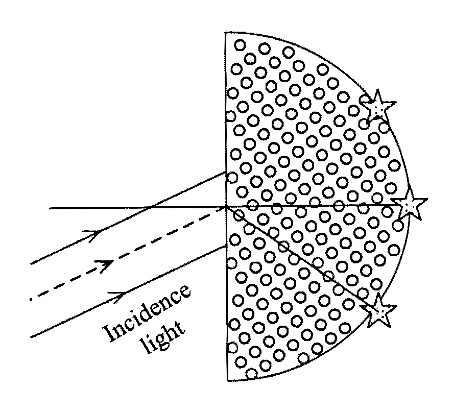
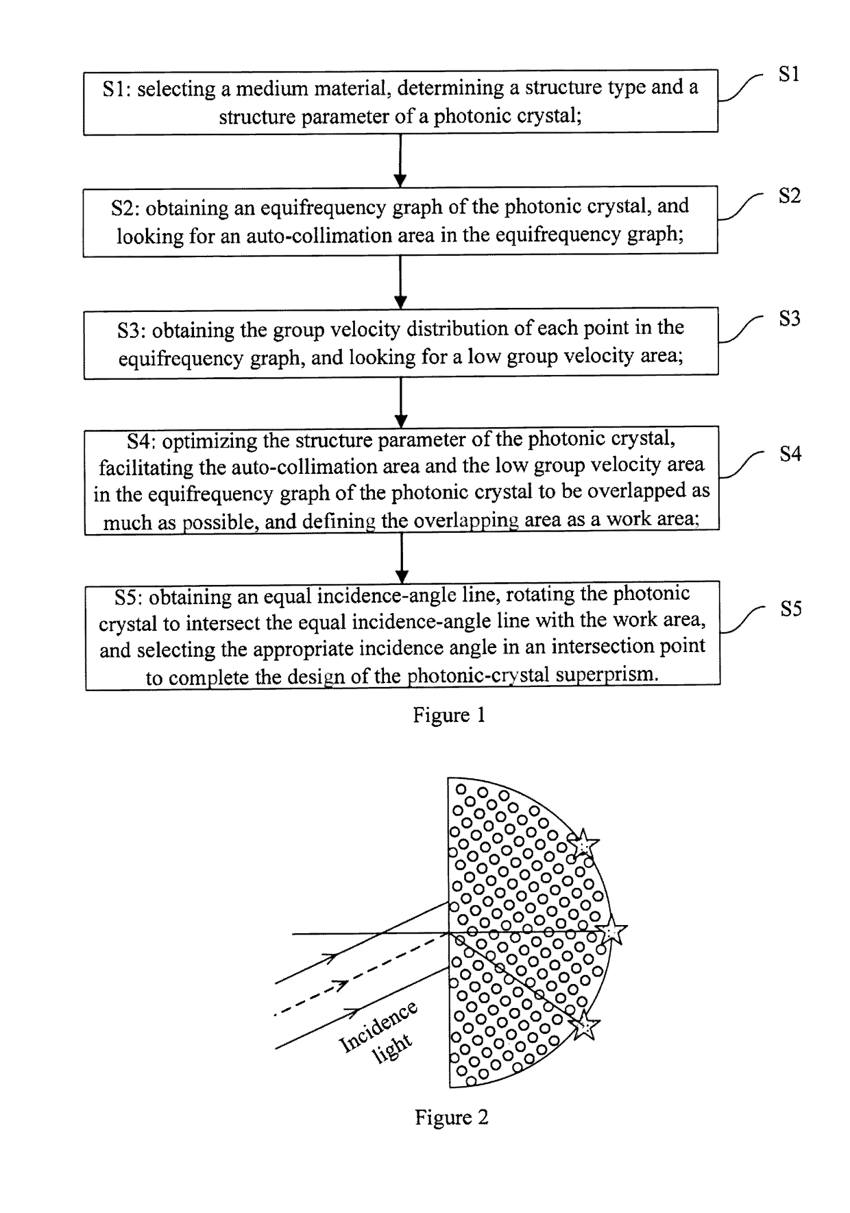
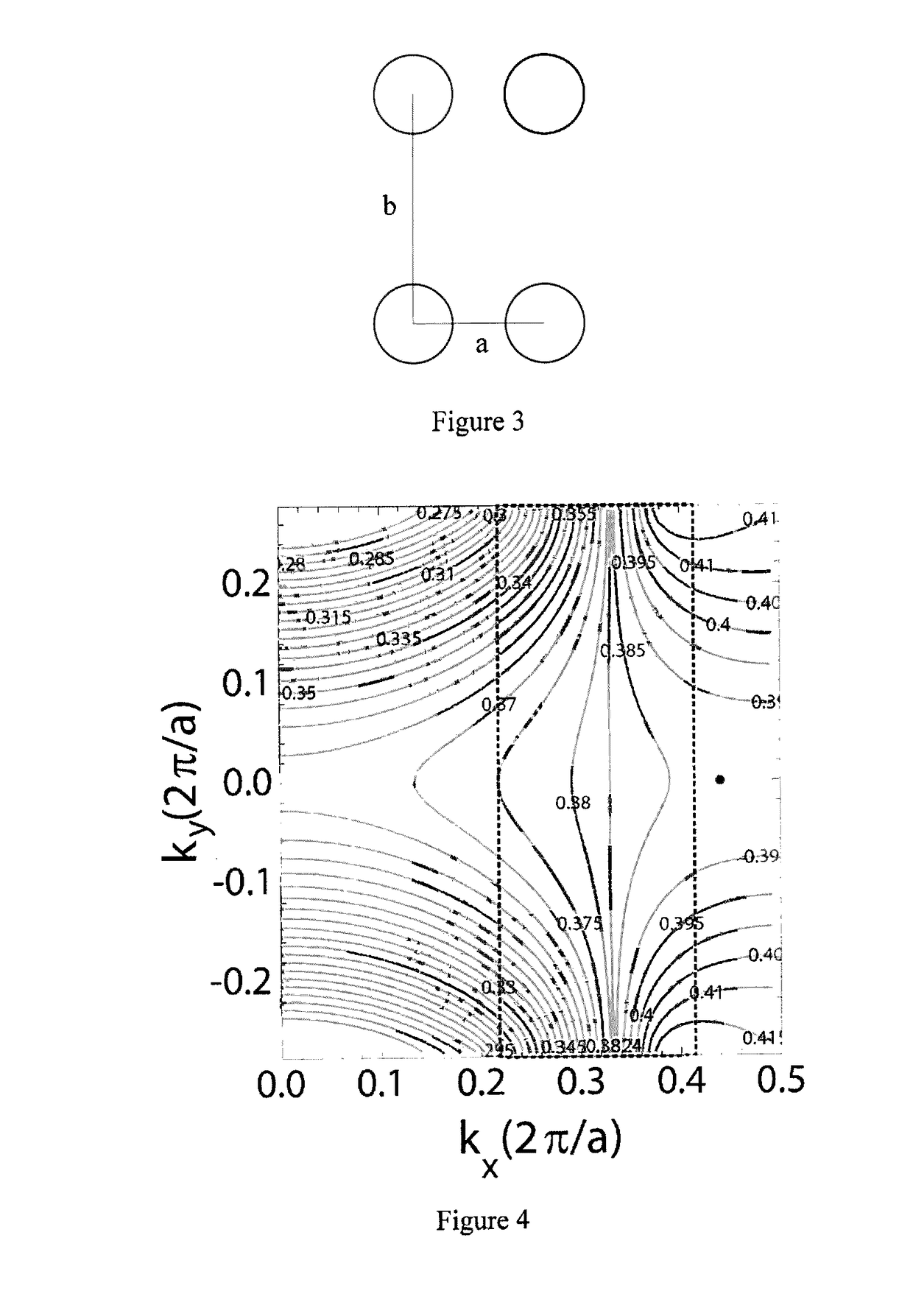
[0036]Please see FIG. 1-FIG. 7c. It shall be noted that the illustrations provided in the present embodiment describe the basic concept of the present invention only in a schematic manner. The figures only show the components related to the present invention instead of being drawn according to the number, shape and size of the components at the time of actual implementation, the type, quantity and proportion of the various components in its actual implementation may be a random cha...


PUM


Abstract

A method for designing an ultrahigh-resolution photonic-crystal superprism, including the following steps: selecting a medium material, and determining a structure type and parameter of a photonic crystal, obtaining the photonic crystal's equifrequency graph, and looking for an auto-collimation area; obtaining the group velocity distribution of points in the equifrequency graph, and looking for a low group velocity area; optimizing the photonic crystal's structure parameter, facilitating the auto-collimation and the low group velocity area in the photonic crystal's equifrequency graph to be overlapped as much as possible, and defining overlapping area as a work area; obtaining an equal incidence-angle line, rotating the photonic crystal to intersect the equal incidence-angle line with the work area, and selecting the appropriate incidence angle in an intersection point to complete the design of the photonic-crystal superprism. When light makes incidence via the above incidence angle, the photonic crystal may separate light with different frequencies significantly.

Description

BACKGROUND OF THE PRESENT INVENTION[0001]Field of Invention[0002]The present invention belongs to the fields of photoelectron and optical communication, and relates to an ultrahigh-resolution photonic-crystal superprism and a method for designing the same.[0003]Description of Related Arts[0004]A photonic crystal was independently proposed by S. John and E. Yablonovitch in 1987, respectively, it is an artificial microstructure formed by mediums which have different refractive indexes with periodically arranging. Because a dielectric constant has periodicity in space, a spatial refractive index is periodically changed. When the change of the dielectric constant is large enough and the period of the change is equal to the wavelength of light, the dispersion relation of light wave will have a band structure, that is, Photonic Band structures. These terminated frequency intervals are called as “Photonic Band Gap” (PBG), light or electromagnetic wave whose frequency falls within a forbidd...

Claims


Application Information

Patent Timeline
Patent Type & Authority Applications(United States)
IPC IPC(8): G02B1/00G02B27/12G02B27/10G02B27/00
CPCG02B1/005G02B27/1006G02B27/126G02B27/0012
Inventor JIANG, XUNYALI, WEIZHANG, XIAOGANGLIN, XULIN
Owner SHANGHAI INST OF MICROSYSTEM & INFORMATION TECH CHINESE ACAD OF SCI
Why Eureka
Try Eureka